Accurate Measuring Systems in Electronics and Semiconductor Industry - View
0 likes | 4 Vues
Step inside the world of precision! This article reveals why accurate measuring systems are critical in electronics and semiconductors. From wafers to PCBs, discover how micron-level accuracy boosts reliability, prevents costly errors, and drives innovation. Learn how VIEW Micro Metrology delivers the precision needed for next-generation technology. Read more https://justpaste.it/d4fqb

Accurate Measuring Systems in Electronics and Semiconductor Industry - View
E N D
Presentation Transcript
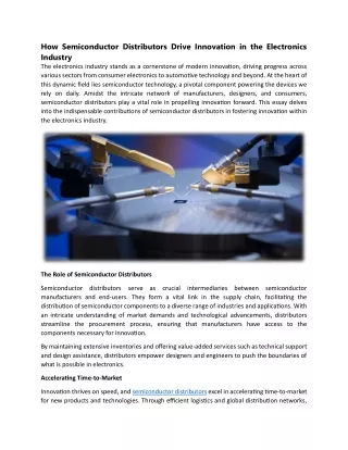
Accurate Measuring Systems in Electronics and Semiconductor Industry The electronics and semiconductor industry operates at the scale of microns and nanometres. At this level, even the smallest measurement error can cause circuit failure, overheating, or reduced product life. This is why accurate measuring systems are essential. They ensure every microchip, wafer, and PCB is built precisely to design standards, supporting performance and reliability in critical devices like smartphones, medical equipment, and aerospace electronics. Why Accuracy Matters in Electronics In semiconductors, a transistor gate may be less than 10 nanometres wide. A slight deviation in etching or deposition can change electrical behaviour. Accurate measuring systems capture real geometry, detect micro-defects, and confirm alignment with CAD models. Example: A PCB with misaligned solder pads can cause short circuits in consumer electronics. High-resolution optical measurement prevents such failures by verifying pad-to- pad spacing.
Key Applications of Accurate Measuring Systems 1. Wafer and MEMS Fabrication During wafer lithography, alignment marks must be measured with sub-micron accuracy. Accurate systems help detect overlay errors, ensuring transistors line up across layers. 2. Chip Assembly and Packaging When dies are mounted onto substrates, the planarity and bond height must be verified. Measuring systems guarantee wire bonds and flip-chip connections remain defect-free. 3. PCB Inspection For printed circuit boards, line width, via size, and solder mask position are inspected. This avoids open circuits or poor connectivity in mass production. 4. Hard Disk Drives and Mobile Devices Read/write heads and micro-lenses require precise alignment. Measuring systems ensure nanometre-level tolerances, extending product reliability. Real-World Insight Leading semiconductor manufacturers in Taiwan and South Korea have reduced product rejection rates by over 20% by integrating inline non-contact measuring systems. These systems identify micro-cracks in wafers before packaging, saving both cost and time. Advantages for Semiconductor Industry ●Micron-to-Nanometre Precision–Essential for today’s ultra-dense circuits. ●Non-Contact Measurement– Prevents damage to delicate wafers and MEMS structures. ●High Repeatability– Same component can be measured multiple times with identical accuracy.
●Process Integration– Inline measurement enables feedback and process control in real time. VIEW Micro Metrology Systems For industries where tolerances are tighter than human hair thickness, VIEW Micro Metrology systems deliver unmatched capability. Whether your work includes wafer and MEMS fabrication, chip test, assembly and packaging (IDM, OSAT, and fan-out wafer-level packaging), photomasks, wire-bonding, PCBs, hard disc drives, mobile devices, or drug delivery systems (implantable, transdermal, intradermal), VIEW systems are engineered to measure components quickly, accurately, and seamlessly within production processes. Key Takeaways: ● Accurate measuring systems prevent micro-defects and enhance product yield. ● Semiconductor packaging and PCB manufacturing rely on nanometre-level tolerance checks. ● Non-contact, inline systems reduce waste and improve process efficiency. To achieve this level of excellence, leading manufacturers turn to VIEW Micro Metrology systems, combining speed, accuracy, and reliability to support next-generation electronics production. Website: www.viewmm.com Mail ID: info@viewmm.com