Download
1 / 38
390 likes | 492 Vues
Explore density of states in 3D, 2D, 1D, and 0D quantum structures, carrier concentrations, energy levels, and wavefunctions. Derive expressions for carrier concentration in conduction and valence bands using Fermi-Dirac distribution.

E N D
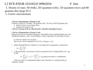
L2 ECE-ENGR 4243/6243 09062016 F. Jain 1. Density of states 3D (bulk), 2D (quantum wells), 1D (quantum wires) and 0D quantum dots [page 85+] 2. Carrier concentrations
Fig. 1. Density of states as a function of energy in bulk, QW, Qwire, Qdot.Calculation of energy levels and wavefunctions in a multiple quantum well layer (pp.30a to 43). Reference: S. Chuang, Chapter 3.
3D Density of States Derivation: We need to have kx= ---(6) The solution depends on boundary conditions. It satisfies boundary condition when Eq.6 is satisfied. Page 52-53: Using periodic boundary condition (x+L) = (x), we get a different solution: If we write a three-dimensional potential well, the problem is not that much different ky = n y= 1,2,3,… kZ = , n z = 1,2,3,…. …(7) The allowed kx, ky, kz values form a grid. The cell size for each allowed state in k-space is …(8)
3-D Density of states as a function of energy in bulk, (15) N(E)dE =
1.8.4 Derivation of carrier concentration expression using density of states in conduction and valence band, and occupancy of electrons and holes using Fermi- Dirac distribution [page 38/ECE 4211] We started this method on page 14. The electron concentration in conduction band between E and E+dE energy states is given by dn = f(E) N(E) dE.To find all the electrons occupying the conduction band, we need to integrate the dn expression from the bottom of the conduction band to the highest lying level or energy width of the conduction band. That is, Eq. 76 This equation assumes that the bottom of the conduction band Ec = 0. Substituting for N(E) the density of states expression, N(E)dE = (58) (84A) An alternate expression results, if Ec is not assumed to be zero. (84B) Another form is n=ni exp[(Ef-Ei)/kT (84C).
1.8.4 Derivation of carrier concentration expression using density of states in conduction and valence band, and occupancy of electrons and holes using Fermi- Dirac distribution [page 38] We started this method on page 14. The electron concentration in conduction band between E and E+dE energy states is given by dn = f(E) N(E) dE.To find all the electrons occupying the conduction band, we need to integrate the dn expression from the bottom of the conduction band to the highest lying level or energy width of the conduction band. That is, Eq. 76 This equation assumes that the bottom of the conduction band Ec = 0. Substituting for N(E) the density of states expression, N(E)dE = (58) (84A) An alternate expression results, if Ec is not assumed to be zero. (84B) Another form is n=ni exp[(Ef-Ei)/kT (84C).
Graphical way to look at 3-D carrier concentrations, pp. 40-41/4211S-15 Figure 28(a) and 28(b) on the following page illustrate the relationship between carrier concentrations and location of the Fermi level with respect to the band edges.In Fig. 28(a) the energy separation (Ec-Ef) between the conduction band edge and the Fermi level Ef is greater than in Fig. 28(b). As a result there are more electrons in case (b), obtained by integrating the dn plot. If n is larger, it means hole concentration is smaller. Similarly, one can plot the situation, when Ef is near the valence edge, now because of the shift of Ef , dp plot will have a larger magnitude, yielding a greater value of hole concentration p than electrons.
AlxGa1-xAs AlxGa1-xAs GaAs V(z) ∆EC ∆Ec = 0.6∆Eg ∆Ev = 0.4∆Eg 0 z 0 ∆EV -EG z ∆EV -EG+∆EV Finite barrier quantum well vs Infinite barrier Well (L1 slide 26) page 70 (15)
C. 2D density of state (quantum wells) page 84 Carrier density in 2-D (quantum well), one dimensional quantization along z- axis. We sum states along kz using quantum number nz (1) Without f(E) we get density of states in 2-D. Number of states per unit area Quantization due to carrier confinement along the z-axis.
1D density of states (quantum wires) p. 85 Carrier density n or p (12) Without f(E) we get density of states Quantization due to carrier confinement along the x and z-axes. Looking at the integration 13 This simplifies 19 Go back to Eq. (12), the density of states in a nano wire is where E=E-Enx-Enz
D. 1D density of state (quantum wires) p85 Carrier density n or p (12) Without f(E) we get density of states Quantization due to carrier confinement along the x and z-axes. Looking at the integration 13 This simplifies 19 Go back to Eq. (12), the density of states in a nano wire is where E=E-Enx-Enz
Density of states in 0-D (Quantum dots)The k values are discrete in all three directions
Energy levels in nanowire (discrete due to nx and nz)Y-axis gives energy width 1. discrete value of nx=1 and then add nz= 1, 2, 3 2. discrete value of nx=2 and then add nz= 1, 2, 3 3. Add to each discrete value of nx, nz an energy width as shown in density of state plot.
Derivation of current due to 1D subband or channel i. [page 91-92] Show conductance quantized as e2/h, g is 2 due to spin (Lecture 3)
Derivation of current due to 1-D subband or channel i. page 91 Show conductance quantized as e2/h, g is 2 due to spin
Application of quantum dots (QDs) in devices Lasers Self assembly of cladded QDs Quantum dot channel (QDC) FETs Quantum dot gate (QDG) FETs Floating gate QD nonvolatile memories (NVMs)
Why quantum well, wire and dot lasers, modulators and solar cells? Quantum Dot Lasers: • Low threshold current density and improved modulation rate. • Temperature insensitive threshold current density in quantum dot lasers. Quantum Dot Modulators: • High field dependent Absorption coefficient (α ~160,000 cm-1) : Ultra-compact intensity modulator • Large electric field-dependent index of refraction change (Δn/n~ 0.1-0.2): Phase or Mach-Zhender Modulators Radiative lifetime τr ~ 14.5 fs (a significant reduction from 100-200fs). Quantum Dot Solar Cells: High absorption coefficent enables very thin films as absorbers. Excitonic effects require use of pseudomorphic cladded nanocrystals (quantum dots ZnCdSe-ZnMgSSe, InGaN-AlGaN) Table I Computed threshold current density (Jth) as a function of dot size infor InGaN/AlGaN Quantum Dot Lasers (Ref. F. Jan and W. Huang, J. Appl. Phys. 85, pp. 2706-2712, March 1999).
Cladding Quantum Dots (QDs) Core • Nanocrystals confined in three dimensions. • Electronic and optical properties of the these particles are dependent on the size and shape of the particles. • The bandgap of the material is inversely proportional to the size of the dot due to the confinement. • Example: Bandgaps of the QDs we prepare in our lab Si QDs – ~1.24 eV where as bulk Si bandgap is 1.17 eV Ge QDs – ~0.91 eV where as bulk Ge bandgap is 0.67/0.69 eV • The mass and mobilities of the electrons in these are effective values and are different from the free electron mass and mobility. 22 Top Ravi[9], below is published results of this research[10]
QDs Colloidal Solution Preparation Intrinsic Powder • 99.999% pure Si/Ge powders. Typical size of the particles with 325 Mesh is ~44 µm. • Perform high energy ball milling for 5 hours. • Mix the ball milled powder with benzoyl Peroxide (oxidative agent ) in ethanol solvent. Sonicate for 48 hours. • Then QDs are separated from the colloidal solution by performing the high-speed centrifuging at 3000, 6000, 9000 and 13000 rpm. • The typical size of the particles obtained here ~20nm with 1-2nm cladding thickness. The size can be further reduced to ~4nm by reoxidizing and etching the cladding layer in 10ppm of 48% hydrofluoric acid and 100% ethanol. Ball Mill Intrinsic Powder Powder + Ethanol + Benzoy Peroxide Keep Solution Sonicated High Sped Centrifuge Reoxidize and Etch
Effect of Ball Milling [1] • Ball milling will reduce the size of micron sized powder particles to nanometers. • Ball milling will change the surface morphology (crystallinity) of the particles. • Ball milling causes the surface amorphization of the Si nanoparticles. • Amorphization will reduce the refractive index and increases the absorption coefficient of the QDs, which causes the change in optical behavior. • Wave number, Where wavelength and n refractive index. • Absorption coefficient , Where absorption coefficient and extinction coefficient of the material 24
Effect of Ball Milling (Cont’d) • Raman spectrum of the Si powder before ball milling (Plot A: c-Si peak at 512 nm) and the spectrum after ball milling (plot B: A-Si peak at 475nm and c-Si peak at 518nm) and the self-assembled Si/SiOx on glass substrate (C). Raman Frequency undergoes a red shift as the diameter of the nanocrystal decreases [2]. Raman investigation suggests that the Si Core in these nanoparticles, 45% of the total Si-atom is composed of 34% crystalline and 11% of amorphous component.
Effect of pH on stability of the QD [1] The Si/SiOx QDs are stable when the pH is between 7.8-6.7. But doesn’t self-assemble on the substrates. When the pH is in between 6.7-4.9 QDs in the solution are not stable will agglomerate/precipitate on the substrate. As the pH is ranging from 4.9 to 3.8 the dots are metastable and self-assemble uniformly on the substrates.
XPS Results [1] From the above the tables we can see the different component suboxides present in the cladding layer and the percent of Si/SiOx in the dot.
Site-Specific Self-Assembly (SSA) [3] Below pH 5 the partial protonation of QD will provide a positive surface charge. P-type substrate will have negative surface charge density. N-type has positive surface density. The positively charged QD will then assemble only on the negative surface charge of P-type substrate
Transport in Quantum dot channel (QDC) FET ID Threshold shift DVTH depends on transfer of charge to the mini-bands (i) in QDSL channel. Vgs Energy mini-bands in SiOx-Si QDSL JEM, 2012. Energy band diagram showing the effect of drain voltage VD in populating upper mini-bands in a QD channel as Vg is increased.
Quantum Dot Gate (QDG) FETs 3-State QDGFET with II-VI gate insulator Cross sectional HRTEM image of QDGFET. Transfer characteristics of a fabricated QDGFET when VDS = 0.5 V Output characteristics of a fabricated QDGFET Karmakar et. al. Journal of Electronic Materials, 40, 2011.
4-State/Mixed-Dot QDG FET 4-State QDGFET with GeOx-Ge and SiOx-Si quantum dots in gate region
Mixed-Dot QDGFET Quantum Simulations Electrons confined in inversion channel when VG = 0V Electrons in lower Ge QDs when VG = 1.0V Electrons tunneled to upper Si QDs when VG = 1.5V Lingalugari et. al. Journal of Electronic Materials, 42, 2013.
QDGFET Experimental Results Transfer characteristics of a fabricated 4-state QDGFET when VD = 0.5 V Output ID-VD characteristics of a fabricated QDGFET with Si and Ge QDs. Lingalugari et. al. Journal of Electronic Materials, 42, 2013.
Results of an Inverter in the SRAM Simulation Results of a 4-state QDGFET based Inverter
Energy band diagram of a floating gate nonvolatile memory(FGNVM) Fig .2. Schematic cross-section of a floating gate nonvolatile memory Fig .4 energy band
References [1] T. Phely-Bobin, D. Chattopadhyay, and F. Papadimitrakopoulos, Chem. Mater., 14, 1030 (2002). [2]C. C. Yang and S. Li, J. Phys. Chem. B 2008, 112, 14193–14197, 2008. [3] F. Jain and F. Papadimitrakopoulos, Patent # 7,368,370 (2008).