Integrated Circuit Design Using Smartphone Audio Output for Efficient Voltage Regulation
This paper presents a novel ASIC CMOS circuit that harnesses a smartphone's audio output to power an integrated circuit at 1.8V and 2mA. Designed for compatibility with both iOS and Android smartphones, the circuit operates efficiently at 37.3%. It fits a compact 1mm x 1mm die with off-chip capacitors. Key components include a rectifier, voltage doubler, charge pump, voltage regulator, and voltage reference. A robust design approach is highlighted, ensuring stability and efficiency.

Integrated Circuit Design Using Smartphone Audio Output for Efficient Voltage Regulation
E N D
Presentation Transcript
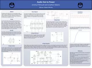
We designed an ASIC CMOS circuit to use a smartphone’s audio output to power an integrated circuit at 1.8 V and 2 mA. The design works on a range of smartphones using iOS and Android operating systems taking into account their varying power outputs at an efficiency of 37.3%. The design can fit on a 1mm x 1mm die with two 2µF and two 1µF capacitors off chip. Abstract Rectifier Voltage Regulator References Milliken, Robert J., Jose Silva-Martinez, and Edgar Sanchez-Sinencio. "Full On-Chip CMOS Low-Dropout Voltage Regulator." IEEE Transactions on Circuits and Systems I: Regular Papers 54.9 (2007): 1879-890. Print. Ker, M.-D., S.-L. Chen, and C.-S. Tsai. "Design of Charge Pump Circuit With Consideration of Gate-Oxide Reliability in Low-Voltage CMOS Processes."IEEE Journal of Solid-State Circuits 41.5 (2006): 1100-107. Print. http://www.ece.gatech.edu/academic/courses/ece4430/Filmed_lectures/BandgapSources/L390-BandgapRefs.pdf Dai, Y., D.T. Comer, D.J. Comer, and C.S. Petrie. "Threshold Voltage Based CMOS Voltage Reference." IEE Proceedings - Circuits, Devices and Systems 151.1 (2004): 58. Print. Cheng, M.-H., and Z.-W. Wu. "Low-power Low-voltage Reference Using Peaking Current Mirror Circuit." Electronics Letters 41.10 (2005): 572. Print. Rogers, Everett. "Stability Analysis of Low-dropout Linear Regulators with a PMOS Pass Element." Weblog post. Web. <http://www.ti.com/lit/an/slyt194/slyt194.pdf>. Weller, Bernhard. "Design and Simulation of a LDO Voltage Regulator." Rpt. inScientific Colloquium. Web. <http://www.arsenal-of-wisdom.org/wp-content/uploads/downloads/2011/02/Des_Sim_LDO.pdf>. Xiong, X. PSPICE Student 9.1 Tutorial. Bridgeport. PDF. Feng, and Tapan. History of the High-Voltage Charge Pump. Professional Engineering 6X9. PDF. The input to the system will be two square waves 180º out-of-phase. A square wave was selected because it transfers the most power. Our design consists of 5 main parts: rectifier, voltage doubler, charge pump, voltage regulator, and voltage reference. Each part was designed and tested separately and then added to the complete schematic. The design process for each part started with reading literature related to the function needed and then choosing which design we would adapt to fit our needs. Next, we built a working schematic of the paper’s model in Cadence Virtuoso in order to decide whether we made the correct choice for design, and then finally adapted it to fit our specific needs. Jeremy O’Driscoll and Jonathan Rubens Advisor: Robert Morley Audio Out to Power Design The rectifier converts the square wave input into two DC waves. This is achieved by selecting which wave is high at any given time and using that as the high output and the same for the low output. We accomplish this with only 4 transistors. The variation on the output at the switching frequency is negligible. Voltage Doubler In order to reach the desired output of 1.8 V, the main line voltage had to be raised from its input level. The voltage doublerideally outputs double the input voltage. This is accomplished by using a switch capacitor, which allows us to have relatively high current output as well as increased voltage. The circuit uses two clocks to operate the switching. This part takes in a wave always greater than 2.2 V and returns a stable 1.8 V DC wave. It is the final part in the main current flow. The circuit works by comparing the output to a reference voltage of 0.9 V and adjusting a pass transistor accordingly until the output is at the right level. The desired output voltage is changed by tweaking the two output resistors. The regulator works by feedback to a comparator and then small changes until 1.8 V is achieved. Stability was a large concern so we had to implement compensation circuitry to slowdown the feedback process. Using this method we achieved 66.3 dB of ripple reduction so that the output is incredibly stable. Charge Pump The charge pump provides the necessary increase in voltage for the clocks of the voltage doubler. To operate correctly, the clocks into the voltage doubler had to be boosted to a higher voltage than the output in order for the transistors to function. This was done with a charge pump design that pushes charge through eight capacitors, multiplying the voltage by four. The small capacitors used cause the component to only function under low current draw, but this works for our design because ideally zero current would flow through the clocks. Voltage Reference This part generates a stable 0.9 V output used in the voltage regulator. The characteristic drop across a MOSFET is used along with a current mirror to provide a stable reference for output. The output changes slightly with temperature, but not enough to make a significant difference at normal operating points. Block Diagram The overall block diagram shows how all the parts connect to form the final product. In addition to the five parts described, there are three inverters which act as amplifiers for clock signals to the voltage doubler. The majority of current will flow from the power source through the rectifier to the voltage doubler and into the voltage regulator. Simulations Ripple Rejection The output of the voltage regulator (in blue) rejects the square wave at the input (in red) with very little ripple. We have achieved 66.3 dB of ripple rejection Input Range The blue curve shows the output voltage of our voltage regulator as a function of the input voltage. It shows that when the input reaches about 2.2 Vthe output will correctly be 1.8 V. This constraint set the output level of our voltage doubler to be at least 2.2 V.