Development of Front-End Electronics for Time Projection Chamber (TPC) at Tsukuba University
This paper presents the development of front-end electronics for a Time Projection Chamber (TPC) designed at the University of Tsukuba. The system includes a printed circuit board (PCB) with 8 analog input channels, FPGA control, and a comprehensive data-taking and analysis program. The TPC serves as a 3-D tracking gas detector, crucial for identifying charged particle trajectories through ionization. We detail the architecture, data flow, and the software for visualization and analysis, with outcomes from prototype tests and future production plans.

Development of Front-End Electronics for Time Projection Chamber (TPC) at Tsukuba University
E N D
Presentation Transcript
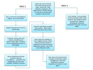
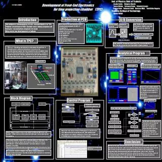
Inst. of Physics. Univ. of TsukubaAsuka Saito. Shigeru Kiuchi.Yasuo Miake. Tatsuya Chujo. Shinichi Esumi. Sumio Kato . Takanori Aoki. Kentaro Miki. Yoshihiko Nagata.Tsukuba College of Technology Motoi INABA Development of Front-End Electronics for time projection chamber(TPC) 9/21/2005 in HAW05 Production of PCB A/D Conversion Introduction Our purpose is development of front-end electronics for TPC. Printed circuit board (PCB), Control data-taking program and Analysis / visualization program are made .We present our development as follows . We designed PCB with following specs: 8 analog input channels (8 ADC’s, 8 Preamplifiers)1 Field programmable gate array (FPGA)100 MHz clock generator 32-bit output port16-bit input port 12-bit I/O portBoard size (18.3cm x 22.5 cm)Board material (FR4)2 layers ADC divides from 0v to 1v into 1024 pieces. If ADC is sent over 1v,ADC send error signal to FPGA. Analog signal from TPC Convert to Digital signal 0001100110 1011011011 AD conversion data What is TPC? divides into 1024 pieces FADC converts the analog signal from TPC to the digital data (10-bit). The data of ten bits sent from FADC is digital signals. TPC is a 3-D tracking gas detector to determine the position of charged particle. When a charged particle ionizes the gas,electrons are made. The electrons drift to wire chamber along electric filed and avalanche is formed near anode wire. It makes a signal on each pad. From the channel of the pad and the timing of the signal, We reconstruct 3-D trajectory of the charged particle. Analytical Program Program language is Visual Basic .net. We develop this program to readout data from the circuit , plot trajectory in 3D image , reconstruction of wave form, and assign color according to amplitude, etc. They are shown below. Image of TPC Channel Map shows signal tension by color Wave form shows a change of signal of one input channel Main screen Electric Field Particle orbit Y Z Cathode pad X Anode Wire Drift of Electron Flight Tracker shows particle trajectory. 2 left screen is plot 2-D . Right screen is plot 3-D.Below figures are method of projection. A red line is a common lone in two figures. Block Diagram Control Program Detector coordinates Z X TPC Trigger Counter PC start The data that came from TPC is preserved in address(n). θ Y Data flow from reading data to display Initialization n←n+1 Observer coordinates Front-end module# 1 Waiting for start-trigger Input run number Y n>1024 Y M=1024 Z X No N PreAMPx 8 FADCx 8 FPGA 3-state buffer Yes Data read Φ Parity bit added M+=1 N=Pad number Y Front-end module# 2 Define two coordinates for a trajectory: one is detector coordinate. another is observer coordinates. Transform the trajectory from one to the other coordinate. Project the trajectory in the observer coordinate. Data is sent to PC. n←1 N=72 M=sampling number N end extract #N Pad data N+=1 Front-end module# 9 When the start signal comes, FPGA begins to take data till 1024 .When data are transferred to PC, ADC address and data address are added. taking data. Since clock frequency is 100 MHz,data are taken each 10 nano seconds . Extract signal intensity , sampling number data Geometric transformation When Trigger counter sends start signal to FPGA on FEM (front-end module), FPGA starts to collect data from ADC and stocks them inside the memory. Plot and Display FPGA sends request signal to PC, after data taking of 1024 data. If PC accepts the request signal, data transfer from FPGA to PC starts.ADC address ( input channel number ) and data address ( signal number ) are added.The parity bit is added in order to judge whether data are correct or not. Conclusion Based on the read-out test with proto-type, we have determined the design and parameters of the front-end circuit board. Production of remaining circuit boards has started. A control and an analysis program as well as 3D visualization programs have been prepared and tested with proto-type circuit. The final verification of the program will be done, when the production is finished. Once all 72 signal channels of TPC are operated, the detector performance (position resolution and efficiency) will be evaluated . Simulation of Verilog HDL for Data taking PC is sent 25-bit per 1 channel . The data of binary notation is converted into the data of decimal notation in PC. The data is recorded in PC as data of 10 digits.