Digital Design Methodology (Revisited)
230 likes | 294 Vues
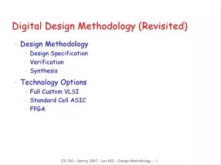
Digital Design Methodology (Revisited). Design Methodology Design Specification Verification Synthesis Technology Options Full Custom VLSI Standard Cell ASIC FPGA. Design Methodology: Big Picture. Postsynthesis Design Validation. Design Specification. Postsynthesis

Digital Design Methodology (Revisited)
E N D
Presentation Transcript
Digital Design Methodology (Revisited) • Design Methodology • Design Specification • Verification • Synthesis • Technology Options • Full Custom VLSI • Standard Cell ASIC • FPGA CS 150 – Spring 2007 - Lec #25 – Design Methodology – 1
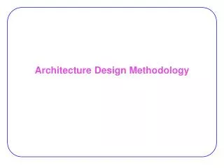
Design Methodology: Big Picture Postsynthesis Design Validation Design Specification Postsynthesis Timing Verification Design Partition Test Generation and Fault Simulation Design Entry Behavioral Modeling Simulation/Functional Verification Cell Placement/Scan Insertation/Routing Verify Physical and Electrical Rules Design Integration And Verification Synthesize and Map Gate-level Net List Pre-Synthesis Sign-Off Design Sign-Off Synthesize and Map Gate-level Net List CS 150 – Spring 2007 - Lec #25 – Design Methodology – 2
Design Specification • Written statement of functionality, timing, area, power, testability, fault coverage, etc. • Functional specification methods: • State Transition Graphs • Timing Charts • Algorithm State Machines (like flowcharts) • HDLs (Verilog and VHDL) CS 150 – Spring 2007 - Lec #25 – Design Methodology – 3
Design Partition • Partition to form an Architecture • Interacting functional units • Control vs. datapath separation • Interconnection structures within datapath • Structural design descriptions • Components described by their behaviorals • Register-transfer descriptions • Top-down design method exploiting hierarchy and reuse of design effort CS 150 – Spring 2007 - Lec #25 – Design Methodology – 4
Design Entry • Primary modern method: hardware description language • Higher productivity than schematic entry • Inherently easy to document • Easier to debug and correct • Easy to change/extend and hence experiment with alternative architectures • Synthesis tools map description into generic technology description • E.g., logic equations or gates that will subsequently be mapped into detailed target technology • Allows this stage to be technology independent (e.g., FPGA LUTs or ASIC standard cell libraries) • Behavioral descriptions are how it is done in industry today CS 150 – Spring 2007 - Lec #25 – Design Methodology – 5
Simulation and Functional Verification • Simulation vs. Formal Methods • Test Plan Development • What functions are to be tested and how • Testbench Development • Testing of independent modules • Testing of composed modules • Test Execution and Model Verification • Errors in design • Errors in description syntax • Ensure that the design can be synthesized • The model must be VERIFIED before the design methodology can proceed CS 150 – Spring 2007 - Lec #25 – Design Methodology – 6
Design Integration and Verification • Integrate and test the individual components that have been independently verified • Appropriate testbench development and integration • Extremely important step and one that is often the source of the biggest problems • Individual modules thoroughly tested • Integration not as carefully tested • Bugs lurking in the interface behavior among modules! CS 150 – Spring 2007 - Lec #25 – Design Methodology – 7
Presynthesis Sign-off • Demonstrate full functionality of the design • Make sure that the behavior specification meets the design specification • Does the demonstrated input/output behavior of the HDL description represent that which is expected from the original design specification • Sign-off only when all functional errors have been eliminated CS 150 – Spring 2007 - Lec #25 – Design Methodology – 8
Gate-Level Synthesis and Technology Mapping • Once all syntax and functional errors have been eliminated, synthesize the design from the behavior description • Optimized Boolean description • Map onto target technology • Optimizations include • Minimize logic • Reduce area • Reduce power • Balance speed vs. other resources consumed • Produces netlist of standard cells or database to configure target FPGA CS 150 – Spring 2007 - Lec #25 – Design Methodology – 9
Postsynthesis Design Validation • Does gate-level synthesized logic implement the same input-output function as the HDL behavioral description? Logic Synthesis Gate-Level Desc Verilog Behavioral Desc Stimulus Generator Testbench for PostsynthesisDesign Validation Response Comparator CS 150 – Spring 2007 - Lec #25 – Design Methodology – 10
Postsynthesis Timing Verification • Are the timing specifications met? • Are the speeds adequate on the critical paths? • Can’t accurately be determined until actual physical layout is understood and analyzed—length of wires, relative placement of sources and sinks, number of switch matrix crosspoints traversed, etc. • Resynthesis may be required to achieve timing goals • Resize transistors • Modify architecture • Choose a different target device or technology CS 150 – Spring 2007 - Lec #25 – Design Methodology – 11
Test Generation and Fault Simulation • This is NOT about debugging the design! • Design should be correct at this stage, so … • Determine set of test vectors to test for inherent fabrication flaws • Need a quick method to sort out the bad from the good chips • More exhaustive testing may be necessary for chips that pass the first level • More relevant for ASIC design than FPGAs • Avoiding this step is one of the advantages of using the FPGA approach • Fault simulation is used to determine how complete are the test vectors CS 150 – Spring 2007 - Lec #25 – Design Methodology – 12
Placement and Routing • ASIC Standard Cells • Select the cells and placement them on the mask • Interconnect the placed cells • Choose implementation scheme for critical signals • E.g., Clock distribution trees to minimize skew • Insert scan paths • FPGAs • Placing functions into particular CLBs/Slices and committing interconnections to particular wires in the switch matrix CS 150 – Spring 2007 - Lec #25 – Design Methodology – 13
Physical and Electrical Design Rule Check • Applies to ASICs primarily • Are mask geometries correct to insure high probability of successful fabrication? • Fan-outs correct? Crosstalk signals within specification? Current drops within specification? Noise levels ok? Power dissipation acceptable? • Many of these issues are not significant at a chip level for an FPGA but may be an issue for the system that incorporates the FPGA CS 150 – Spring 2007 - Lec #25 – Design Methodology – 14
Parasitic Extraction • Extract geometric information from design to determine capacitance • Yields a much more realistic model of signal performance and delay • Are the speed (timing) and power goals of the design still met? • Could trigger another redesign/resythesize cycle if not met CS 150 – Spring 2007 - Lec #25 – Design Methodology – 15
Design Sign-off • All design constraints have been met • Timing specifications have been met • Mask set ready for fabrication CS 150 – Spring 2007 - Lec #25 – Design Methodology – 16
SIA Roadmap—Technology Trends 2006 0.07 mm 40 million 1000 mm2 2009 0.05 mm 64 million 1100 mm2 2012 0.035 mm 100 million 1300 mm2 1999 0.14 mm 14 million 800 mm2 2001 0.12 mm 16 million 850 mm2 2003 0.10 mm 24 million 900 mm2 Transistor Gate Length Transistors per cm2 Chip Size CS 150 – Spring 2007 - Lec #25 – Design Methodology – 17
Alternative Technologies • Standard Chips • Commonly used logic functions • Small amount of circuitry, order 100 transistors • Popular through the early 1980s • Programmable Logic Devices • Generalized structure with programmable switches to allow (re)configuration in many different ways • PALs, PLAs, FPGAs • FPGAs go up 10+ million transistors • Widely used today • Custom-Designed Chips • Semi-custom: Gate Arrays, Standard Cells • Full-custom CS 150 – Spring 2007 - Lec #25 – Design Methodology – 18
Comparison of Implementation Technologies • Full Custom Chips • Largest number of logic gates and highest speed • Microprocessors and memory chips • Created from scratch as a custom layout • Significant design effort and design time • Standard Cell (ASIC) Variation • Gate arrays: prefab’d gates and routing channels • Can be stockpiled • Customization comes from completing the wiring layer • Library cells: predesigned logic, custom placed and routed • All process layers are fabricated for a given design • Design time is accelerated, but implementation time is still slow CS 150 – Spring 2007 - Lec #25 – Design Methodology – 19
Comparison of Implementation Technologies • Field Programmable Gate Arrays • Combines advantages of ASIC density with fast implementation process • Nature of the programmable interconnect leads to slower performing designs than that possible with other approaches • Appropriate for prototyping, where speed to implementation is the key factor (CS 150!) • Or where density is important but the unit volumes are not large enough to justify the design effort and costs associated with custom-designed approaches CS 150 – Spring 2007 - Lec #25 – Design Methodology – 20
Alternative Technologies for IC Implementation Market Volume to Amortize Full Custom IC Standard Cells Time to Prototype FGPAs Gate Arrays PLDs Nonrecurring engineering cost Process Complexity Density, speed, complexity CS 150 – Spring 2007 - Lec #25 – Design Methodology – 21
Die Photos: Vertex vs. Pentium IV • FGPA Vertex chip looks remarkably well structured • Very dense, very regular structure • Full Custom Pentium chip somewhat more random in structure • Large on-chip memories (caches) are visible CS 150 – Spring 2007 - Lec #25 – Design Methodology – 22