Explore Nanotechnology: From Nanostructures to Clean Rooms
Discover the world of nanotechnology, from nanostructures like carbon nanotubes to clean room fabrication processes. Learn about top-down and bottom-up fabrication methods, self-assembly techniques, and the importance of chemistry in creating nanoscale devices. Dive into the intricate world of building things at the atomic scale!

Explore Nanotechnology: From Nanostructures to Clean Rooms
E N D
Presentation Transcript
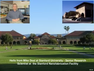
Hello from Mike Deal at Stanford University - Senior Research Scientist at the Stanford Nanofabrication Facility V5.15
Nanotechnology “Nano” – From the Greek word for “dwarf” and means 10-9, or one-billionth. Here it refers to one-billionth of a meter, or 1 nanometer (nm). 1 nanometer is about 3 atoms long. “Nanotechnology” – Building and using materials, devices and machines at the nanometer (atomic/molecular) scale.
Nanostructures Carbon nanotube Gold/Silver nanoparticle (U. Notre Dame) Intel’s transistors used in their integrated circuits (computer chips)
How do you build something so small? “Top-down” – building something by starting with a larger piece and carving away material (like a sculpture). “Bottom-up” – building something by putting together smaller pieces (like building a car engine). Chemistry is important in both top-down and bottom-up processes
Bottom-up fabrication • Adding atoms to atoms, molecules to molecules • “Self-assembly” of atoms and molecules • Use of chemical and biological processes • Current day examples: Self-assemble of organic monolayers for molecular transistors, etc. (Yale) Carbon Nanotubes Vertical growth of nanowires for electronic devices (Stanford) More extreme example: Self-replicating robots.
Top-down fabrication Method used by integrated circuit industry to fabricate computer chips down to ~ 15 nm size • Makes use of depositing thin films, then “photolithography” and plasma etching to make films into desired patterns on a silicon wafer.
“Top-Down” nanofabrication Silicon wafer
Deposition equipment Silicon wafer
Deposition equipment Gas phase reactants Silicon wafer
Deposition equipment Gas phase reactants SiN film Silicon wafer
SiN film Silicon wafer
Photo-sensitive layer (“photoresist”) SiN film Silicon wafer
Photolithography equipment Light source “mask” Photo-sensitive layer (“photoresist”) SiN film Silicon wafer
Photolithography equipment Light source Ultraviolet light “mask” Photo-sensitive layer (“photoresist”) SiN film Silicon wafer
Photolithography equipment Light source Ultraviolet light “mask” Photo-sensitive layer (“photoresist”) SiN film Silicon wafer
Photo-sensitive layer (“photoresist”) SiN film Silicon wafer
Chemical developer Photo-sensitive layer (“photoresist”) SiN film Silicon wafer
Chemical developer Photo-sensitive layer (“photoresist”) SiN film Silicon wafer
Photo-sensitive layer (“photoresist”) SiN film Silicon wafer
Etching equipment Plasma gas (etches film) Photo-sensitive layer (“photoresist”) SiN film Silicon wafer
Etching equipment Plasma gas (etches film) Photo-sensitive layer (“photoresist”) SiN film Silicon wafer
SiN film Silicon wafer SiN thin film patterned correctly!
With contamination present Starting at photoresist step: Photo-sensitive layer (“photoresist”) SiN film Silicon wafer
With contamination present Dust particle Photo-sensitive layer (“photoresist”) SiN film Silicon wafer
With contamination present Light source Ultraviolet light “mask” Photo-sensitive layer (“photoresist”) SiN film Silicon wafer
With contamination present Photo-sensitive layer (“photoresist”) SiN film Silicon wafer
With contamination present Another dust particle Photo-sensitive layer (“photoresist”) SiN film Silicon wafer
With contamination present Plasma gas (etches film) Photo-sensitive layer (“photoresist”) SiN film Silicon wafer
With contamination present Photo-sensitive layer (“photoresist”) SiN film Silicon wafer SiN thin film patterned incorrectly!
How do you build something so small? • Requires very clean environment: “clean room” Magnified image of contaminant on wafer surface, which can cause defects and failures in nanostructures Relative size of clean room contaminants
How do you build something so small? • Requires very clean environment: “clean room” • People wear clean room suits (also called “gowns” or “bunny-suits) • Huge fans circulate filtered air throughout the facility • Wafers are cleaned in liquid solutions between every processing step A lab user “gowning-up” in SNF
Gregory Book and Swaminathan Rajaraman (Swami) at Georgia Tech University Greg Haugstad at University of Minnesota

