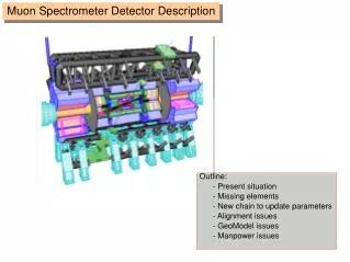
Muon Collider Detector
Muon Collider Detector. “New Instrumentation Possibilities. MCD – Progress Since Snowmass96. None But an enormous amount of Detector R&D has been done LHC ILC CLIC (really ILC’) What is Most relevant to the MCD are developments for ILC detectors


Muon Collider Detector
E N D
Presentation Transcript
Muon Collider Detector “New Instrumentation Possibilities
MCD – Progress Since Snowmass96 • None • But an enormous amount of Detector R&D has been done • LHC • ILC • CLIC (really ILC’) • What is Most relevant to the MCD are developments for ILC detectors • Same physics, especially when we compare to CLIC Alan Bross BNL Muon Collider Design Workshop December 4, 2007
Major Issues • Event Rates • Not really an issue, LHC detector/electronics developments can easily handle MC event rates • Backgrounds, radiation-damage effects are what need to addressed Alan Bross BNL Muon Collider Design Workshop December 4, 2007
Snowmass 96 Background Calculations Alan Bross BNL Muon Collider Design Workshop December 4, 2007
Snowmass 96 Background Calculations II Longitudinal Radial Alan Bross BNL Muon Collider Design Workshop December 4, 2007
Snowmass 96 Detector Alan Bross BNL Muon Collider Design Workshop December 4, 2007
Snowmass 96 Detector II • Central Magnet • 2T • » 8 X 15 m • SVD • 300 mm cell • 300 mm thick • TPC Central Tracker • Cal • LAr • Scintillator Tiles • Muon • Cathode Strips/pads Alan Bross BNL Muon Collider Design Workshop December 4, 2007
Snowmass 96 Detector II • Central Magnet • OK • CMS, 4T, 6X12.5m • MCD, 2T, 8X15m (probably 4T is affordable) • SVD • Occupancy OK – 3% (» 30 hits/cm2) • Radiation damage (n) – Marginally OK (conservative – Not OK) • 1 Year lifetime (1014 n/cm2) • TPC • Probably would work even with 1996 technology • Calorimetry • Also Probably OK • Muon System • OK Alan Bross BNL Muon Collider Design Workshop December 4, 2007
Developments in last 10 Years • Lets Look at ILC/CLIC • CLIC IR: Beamstrahlung (dB) » 20% » 6o Alan Bross BNL Muon Collider Design Workshop December 4, 2007
CLIC Detector Performance Criteria/Goals Alan Bross BNL Muon Collider Design Workshop December 4, 2007
Track Density at CLIC Snowmass 96 MCD = 30/cm2 @ 10 cm Alan Bross BNL Muon Collider Design Workshop December 4, 2007
ILC RDR – Volume 4: Detectors • 325 Participating Institutions! Alan Bross BNL Muon Collider Design Workshop December 4, 2007
ILC RDR – Volume 4: Detectors No one has been able to determine how many contributors Alan Bross BNL Muon Collider Design Workshop December 4, 2007
ILC Detector R&D • An enormous amount of work has been done over the last 10 years • Much is directly relevant to a MCD • What follows has been graciously supplied by Marcel Demarteau, the Fermilab ILC Detector R&D Leader Alan Bross BNL Muon Collider Design Workshop December 4, 2007
ILC Detector R&D Marcel DemarteauFermilab TWEPP07 – Prague, September 7, 2007
~199 ms 969 ms 969 ms Some ILC Parameters • Time structure • five trains of 2625 bunches per second • bunch separation is 369.2 ns (LEP: 22 ms) • Readout options driven by physics • Once per train; time stamping sets time resolution • Once per bunch • Duty cycle (1 ms of data – 199 ms idle) allows for “power pulsing” • Switch power to quiescent mode during idle time • Single IR with 14 mrad crossing angle • Beam size: sx = 640 nm, sy = 6 nm
Specification for an ILC Detector • ILC detectors are precision detectors: fully reconstruct the final state over the full angular region • Identify each and every particle, with high efficiency and high purity, over the full angular range • Differentiate between Z’s and W’s in their hadronic decay • Differentiate between b- and c-quarks • Differentiate between b- and anti-b quark • Although these requirements are common drivers for all experiments, they are non-negotiable requirements for the ILC !
The ILC Concept Detectors • Requirements: LDC GLD SiD 4th • Impact parameter resolution: • Momentum resolution: • Jet energy resolution:
Calorimetry • Goal: s(E)/E ~ 3-4% • Ability to separate Z → qq from W → qq’ • Paradigms: • Dual or Triple Readout • Particle Flow Algorithm (PFA) • Enabling Technologies: • New generation of Photon Detectors • Highly integrated microelectronics • Strategies: • Digital versus Analogue readout H1 ATLAS (Ejet) (GeV) * ALEPH Goal for PFA-ILC Ejet ( GeV)
Multiple Readout Calorimetry • Dual-Readout: measure every shower twice • Scintillation light: from all charged particles • Čerenkov light: b=1 particles, mainly EM • By measuring separately both componentscan determine e/h fraction and correct the response (set e/h=1) • Approaches: • Scintillating and quartz fibers embedded in Cu (DREAM); • no longitudinal segmentation • Leadglass-Scintillator sampling • Doped crystals DREAM200 GeV p
Particle Flow Algorithm • The other paradigm to obtain better energy resolution: PFA • PFA: Reconstruct momenta of individual particles in jet; avoid double counting • Measure photons in the ECAL • Measure charged particles in the tracking system • Subtract calorimeter energy associated with charged hadrons • Measure neutral hadrons in the HCAL (+ ECAL) • PFA: a brilliant idea ! • Novelty is in reducing the role of the hadron calorimeter – and thus the hadron energy resolution – to the measurement of neutral hadrons only • Implications for the calorimetry • Granularity, longitudinal and transverse ! • Sampling of the hadron calorimeter • Digital or analog readout Imaging calorimeter
Calorimeter Architectures • One of the main drivers for imaging calorimeters is granularity • Need to separate energy deposits from different particles
Analogue Electromagnetic Calorimeter • Silicon-Tungsten sampling calorimeter • Total Si area (incl. endcaps) ~2000 m2 • Total number of channels up to 80×106 • Average dissipated power 1-4 μW/mm2 • LDC approach: • Sensitive silicon layers are on PCBs • 1x1cm2 pads, ~1.5m long × 30cm wide • Pad readout digitized to ~16 bits by VFE ASIC • SiD approach: • 6” hexagonal wafers with 1024 13 mm2 pixels • Readout with one ASIC, connected to readout cable • Scintillator-Tungsten sampling calorimeter • GLD approach: • Tile and strip configuration • WLS fiber readout with Photo-detector
Digital Electromagnetic Calorimeter • EM calorimeter based on Monolithic Active Pixel Sensors • Intrinsic high granularity through wafer processing • CMOS process cheaper than high resistivity pure silicon • ECAL MAPS design • Binary readout, threshold adjustment for each pixel • Pixels 50μm×50μm, 4 diodes for Charge Collection • With ~100 particles/mm2 in the shower core and 1% prob. of double hit the pixel size should be ~40 μm×40 μm • Prototype device with two types of readout • Time Stamping with 13 bits (8192 bunches) • Hit buffering for entire train, readout between trains • Capability to mask individual pixels • Total number of ECAL pixels around 8×10¹¹: Terapixels 50 mm • Device being simulated • Signal to Noise > 15 for 1.8 µm Diode Size • Critical issue for Terapixel system
Analogue Hadron Calorimeter • Planes of scintillator and absorber: GLD: z/x/T; LDC: tiles only • Very high granularity • 4x4cm2x5mm; 1x20cm2x5mm (GLD) • 3x3 / 6x6 / 12x12 cm2 tiles (Calice) • Each element read out separately • Massive number of readout channels ~50M channels • Photon detection of scintillator light • Collection through WLS fiber • Direct coupling of detector on scintillator • Enabling technology: Geiger-mode Avalanche Photo Diodes
Geiger-mode Avalanche Photo Diode • The technology that enables this high granularity is Geiger-mode Avalanche Photo Diodes (MRS, MPPC, SiPM, PPD) • Array of pixels connected to a single output • Signal = Sum of all cells fired; binary device ! • If probability to hit a single cell < 1 Signal proportional to # photons • Characteristics: • Pros • Very compact • High PDE (15~20% for 1600 pix) • Insensitive to magnetic field • High gain (105~106) • Operational at Vbias=70~80 V • Good timing resolution • Cons • Thermal noise rate (100kHz~300kHz @ 0.5 pe) • Response is non-linear due to limited number of pixels (saturation effect) • Sensitive to temperature change • Cross-talk and after-pulsing • Vendors • Hamamatsu, SensL, IRST, Mephi, Pulsar, CPTA/Photonique, Dubna/Mikron, Kotura, aPeak, … IRST 1mm 1mm 3x3x0.5 cm3UNIPLAST1 mm WLS Kuraray fiber Y11(300)
Signal path Mylar Signal Pad(s) Fishing line Glue Resistive paint Channel Glass Gas volume Mylar HV Glass Digital Hadron Calorimetry • Three technologies: • Resistive Plate Chamber (RPC) • Single gap • Coated glass as resistive plates • Avalanche mode • Readout pads ~1x1 cm2 • Gas Electron Multiplier (GEM) • Separate drift and amplif. gap • Aiming at ~1x1cm2 readout • Micro MEsh GAseous Structure • Fine mesh separates 3mm drift and 0.1mm amplification gaps • R&D • Performance metrics • MIP detection efficiency uniformity • Readout multiplicity • Noise rate, rate capability • Gain experience in large scale and long-term operation and production • Identify critical operational issues RPC GEM Padboard
Tracking • Goal: • Superb momentum resolution • Robust pattern recognition and good two track separation • Tolerant to high machine background • Paradigms: • Silicon Tracking • •superb position resolution • •compact tracker • Time Projection Chamber (TPC) • many space points (~200) • Two track resolution <2/5-10mm (r,f)/(r,z) • Enabling Technologies: • Advances in Si processing • Precision TPC readout
ALICE TPC dp/p 1%, B=0.4T Material 3.5% X0 near = 0 MWPC readout, ~500k cathode pads, pad sizes 4x7.5, 6x10, 6x15 mm2 hit resol. 800 … 1250 m r, z ILC TPC dp/p 0.1%, B=4T Material <3% X0 near = 0<30%X0 endcap pads per endcap > 106, pad size about 1x6 mm2 hit resol. 100, 500 m r, z @ 4T Readout GEM MicroMegas CMOS Pixels TPC Tracking
GEM MicroMegas TPC Readout Anode Anode • micromesh sustained by pillars • amplification between mesh and pads/strip plane • single stage • 50 mm amplification region includes the anode • Now “Bulk Micromegas” can be obtained by lamination of a woven grid on an anode with a photo-imageable film • The ILC-TPC resolution goal, ~100 µm for all tracks, appears feasible. • two copper foils separated by polyimide • uses 2 or more stages for safer operation • high electric field inside the holes, in which multiplication takes place • 50 mm amplification region is displaced from the anode MicroMegas, 2x6mm2 padsB=1T
TPC CMOS Readout • Use bare CMOS chip as anode to directly collect signals from GEMs or Micromegas: MediPix chip • Charge collection with granularity matching primary ionization cluster spread • On-chip processing of signals • Currently: • 3rd coordinate (time) being added: TimePix chip • Integration of GEM/Micromegas grid and CMOS sensor through wafer processing (InGrid) • Prospects: • Ionization cluster counting is possible to improve part. id. performance • Potential for large improvements in pattern recognition and dE/dx • “Digital Bubble Chamber” GEM foil integrated on chip
TPC R&D • Many prototype TPC’s built • Interchangeable gas-amplification • Wide range of studies: • Gas and resolution studies • Candidate gas amplification devices • Direct comparison of triple-GEM and Bulk Micromegas • Ion/electron transmission studies • Ion feedback measurements • Plan for large prototype TPC • 60 cm drift length, 80 cm diameter • Interchangeable gas-amplificationmodules designed to directly compare gas-amplification technologies • Need for large bore high magnetic field! • R&D synergistic with T2K • T2K will have 3 TPCs • 72 Micromegas modules • Total area ~ 9 m2 • 124416 readout channels Cornell/Purdue small prototype Large TPC D=80cm
SET ECT SIT FTD LDC Silicon Tracker • All silicon tracking, SiD • “Power-pulsing” allows for gas cooling • Hybrid-less design • 100x100mm2 sensor from 6” wafer with 1840 (3679) readout (interm.) strips • Integration of pitch adapter through 2nd metal layer in sensor for signal routing • Sensor (1840 channels) read out with two asics (kPix) • Power and clock routed over the sensor ! • Silicon as “ intermediate layers” • Double-sided layers to act as tracker • d-s silicon R&D actively being pursued in Korea • Single-sided layers to “link” subdetectors • Long-ladders with associated FE Asic SiD
Vertexing • Goal: • Superb impact parameter resolution • Minimal material budget: < 0.1%X0 / layer • Equivalent to 100 mm of Silicon • Minimal power consumption (<50W) • Ability to determine quark charge • Tolerant to high machine background • Paradigms: • Readout during the train • Readout in-between trains
ILC Candidate Technologies • CCD’s • Column Parallel (UK) • Fine Pixel (Japan) • ISIS (UK) • Split Column (SLAC) • CMOS Active Pixels • Mimosa series (Ires) • INFN • LDRD 1-3 (LBNL) • CAP 1-4 (Hawaii) • Chronopixel (Oregon/Yale) • SOI • American Semiconductor/FNAL • LDRD-SOI (LBNL) • CAP5 (Hawaii) • OKI/KEK • 3D • VIP (FNAL) • DEPFET (Munich) CPC2 ISIS LBL-LDRD3 MIIMOSA-n CAPS4 3D DEPFET
Sensor Architectures • An incomplete attempt at listing some of the current architectures design for ILC pixel detectors • With apologies to all other technologies, I will only mention three: CP-CCD, Mimosa, 3D
M N Column Parallel CCD Readout time = N/fout Column Parallel CCD • CP-CCD: read out a vector instead of a matrix • Readout time shortened by orders of magnitude • But every column needs its own amplifier and ADC: readout chip • Need to operate at 50 MHz to meet ILC readout rate spec. • Driving of CP-CCD is a major challenge • 2nd generation large area sensors : CPC2 • Devices with 2-level metal clock distribution • 25 μm and 50 μm epi layers • Reaches 45 MHz operation (designed for 50 MHz) • Dedicated readout chip • CPR2, bump bonded at VTT to CPC2 • Dedicated clock drive chip • CPD1, requirement of 2 Vpk-pk at 50 MHz over 40 nF CPR2 CPC2
Mimosa • Mimosa-16 being developed as beamline telescope for DESY (and Fermilab) testbeam: • Column parallel readout • 32 // columns of 128 pixels (pitch: 25 µm) • ~11–16 µm epitaxy • on-pixel CDS • Final geometry: • 1024 columns of 512 pixels, 20 µm pitch • Expected hit resolution < 2.5 µm • Sensitive area = 20.48 x 10.24 mm2 • pixels with integrated CDS • sensor with integrated 4/5-bit ADC • possibly zero-suppression • Read-out speed • default tr.o. = 512 lines / 5 MHz ~ 100 µs • Possible variant • 1280 columns of 640 pixels, 16 µm pitch with binary readout
Vertical Integration – 3D • A 3D device is a chip comprised of 2 or more layers of semiconductor devices which have been thinned, bonded, and interconnected to form a monolithic circuit • Advantages of 3D • Increased circuit density due to multiple tiers of electronics • Fully active sensor area • Independent control of substrate materials for each of the tiers • Process optimization for each layer • Ability to mate various technologies in a monolithic assembly • Technology driven by industry • Reduce R, L, C for higher speed • Reduce chip I/O pads • Provide increased functionality • Reduce interconnect power, crosstalk • Critical issue are: • Layer thinning to < 10 mm • Precision alignment (< 1 mm) • Bonding of the layers • Through-wafer via formation
Tier 38.2 µm 3D Via Tier 27.8 µm oxide-oxide bond Tier 16.0 µm Buried Oxide(BOX) 400 nm thick 2000 ohm-cm p-type substrate VIP Chip • 3D chip Vertical Integrated Pixel (VIP) chip submitted by Fermilab to DARPA funded MIT-LL 0.18 mm 3D process • Chips due to arrive in a couple of weeks; key features: • Analog pulse height, sparse readout, high resolution time stamp, front-end power ~ 1875 mW/mm2 (before cycling), 175 transistors in 20x20 µm2 pixel.
Sensor Technology • Device thinning is becoming very common • CCD’s are regularly thinned to 20 mm • LBL has thinned over 15 Mimosa CMOS MAPS chips down to 40 mm • Yield of functional chips ~90% • Studies of charge collection and S/N before/after back-thinning • Some evidence of small signal loss after thinning • Sensors will be used in Fermilab beam telescope • Fermilab has thinned BTeV Fpix chips/wafers to 15/20 mm with ~75% yield • Thinned Edgeless Sensors • Sensors sensitive to the edge can be fabricated by a combination of trench etching, thinning, and laser annealing • Fermilab producing a set of detectors thinned to 50-100 mm at MIT-LL for beam and probe tests Detector bias 20 mm To other pixels Diode implants Trench on detector edge filled with poly and connected to bottom implant Implant with laser annealing Detector Cross section near one detector edge
Conclusions • For the most part, currently available or developing technology will meet the performance criteria as stated in Snowmass 96 for • Muon System • Calorimetry • Central Tracking (r>20-50 cm) Non-Silicon • However, neutrons could still be a problem for readout electronics. For a TPC option, for example, front-end electronics at the end planes would have to be shielded from low-energy neutrons (longitudinal fluence) • Inner Tracking (Vertexing) presents problems due to the large n fluence Alan Bross BNL Muon Collider Design Workshop December 4, 2007
Conclusions II • Vertexing example: CMS Pixels (@ r=4.3cm) • » 2 X 10¹⁴ n for 5 years of running @1034 cm-2s-1 • Lifetime limit • Options • Thinner detectors • 40 mm vs. 300 (X8) • Amorphous Si • CVD Diamond detectors • ~ X100 hardness over Si • LARP Detector R&D • Prototype Diamond detector system (pixel luminosity telescope (PLT) for CMS NIEL Non-Ionizing Energy Loss Alan Bross BNL Muon Collider Design Workshop December 4, 2007
Conclusions III • Ongoing detector R&D (ILC, LARP) is addressing many detector issues for the MCD • First order of business - Need • Next iteration on interaction region design • Next iteration on collider ring design • May ameliorate some of the radiation background problems • The outcome of these design studies can then be used as input to a new round of radiation background studies for the MCD • Lead to directions for dedicated detector R&D for the MCD Alan Bross BNL Muon Collider Design Workshop December 4, 2007