Assembly and Packaging 2009
International Technology Roadmap for Semiconductors. Assembly and Packaging 2009. Assembly and Packaging Technical Working Group Participants and Collaborators for 2009. 86 Members Representation from: Europe Japan Korea Taiwan United States Hong Kong

Assembly and Packaging 2009
E N D
Presentation Transcript
International Technology Roadmap for Semiconductors Assembly and Packaging 2009
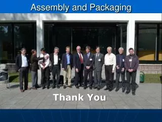
Assembly and Packaging Technical Working Group Participants and Collaborators for 2009 • 86 Members • Representation from: • Europe • Japan • Korea • Taiwan • United States • Hong Kong • Meeting in Beijing for input from China • Active Collaboration with iNEMI and JISSO Roadmaps • Joint Project with MIT Microphotonics Center
Major Activities 2009Revision made to single chip package categories Previous Categories New Categories
Major Activities 2009 Expanded coverage of : • Wafer Level Packaging • Wafer thinning, singulation and bonding for 3D integration • Optoelectronics • Through silicon vias Added coverage of: • Photovoltaics • LEDs • Power devices
Cross TWG Activity • ERM-new materials • Design-3D co-design • Wireless-MEMS • Test-probably good die • ESH- information on regulatory concerns • Yield- yield analysis and optimization tools for packaging (WLP first) • Interconnect (3D Integration)
Automotive Packaging The rapid growth in hybrid and electric vehicles brings an additional class of electronics and a new subset of environmental conditions that are addressed in the 2009 Roadmap.
Major Activities 2009 Major revisions to tables for: • Optoelectronics • System in Package • Wafer thinning • Wafer level Packaging • Wafer Stacking/3D integration
Major Activities 2009 New tables for: • Photovoltaics • Power devices • Packaging gaps and needs • Optical Transceivers • Packaging Consortia
Cu interconnect Ultra Low k dielectrics High k dielectrics Organic semiconductors Green Materials Pb free Halogen free But improvements are needed New Materials will be requiredWorking with ERM the Needs have been identified Many are in development Many are in use today • Nanotubes • Nano Wires • Macromolecules • Nano Particles • Composite materials
Functional Diversification and “More than Moore” are driving rapid change in Packaging Technology Everything is changing: • Architectures • Materials • processes • equipment
ITRS Assembly and Packaging TWG and MIT’s Microphotonics Center are Collaborating on 3DImplementation of a Computing SiP This project is intended to identify the difficult challenges and potential solutions for Complex 3D integration with SiP
The Target is Tera-scale computing by 2015 • Implementation of a 3D Integrated Computing SiP targeting Capability in 2015 • This Project illustrates the technical challenges for packaging posed by technology nodes below 45nm
Tera-scale Computing by 2015 TSV die to die connection 200GB; 500GB/s memory (20 sectors at 25GB/s) Silicon Interposer with: -Integrated thermal management -Integrated Passive networks Memory Memory Memory cube 1Tbyte; 500GB/s (20 sectors at 25GB/s) Interposer Processor Memory Processor Memory Interposer Memory Processor Interposer Processor Memory Interposer Memory Processor Memory Processor Interposer Memory Interposer Processor Memory Processor Memory Optical channel Interposer Memory Processor Processor System in Package Substrate With CNT based heat spreader Processor with 1000 cores/10 layers Core transistor speed 1GHz 25um thick wafer (~400mV power) 1TB/s optical transceiver for: - Off package communication - On package routing
Tera-scale Computing by 2015Collaboration underway to identify challenges and define solutions ITRS Technical working subgroups are addressing: • TSV technology • Thermal management • Die to die bonding • Power integrity • SiP integration • Optical signaling • Package substrate requirements
Significant Gaps Remain Packaging Technology is experiencing a wave of innovation but significant gaps and unresolved technology needs remain which are summarized in the following slides
Better understanding of interfacial science of adhesion / delamination of packaging materials and interfaces in use today is needed. This area is one of the key areas that will impact future yield and reliability. • Through Silicon Via development and productization needs • acceleration. • Key issues: • high throughput processes and equipment • high integrated yield • reliability data • design rules availability and cost
Package warpage at elevated temperature (SMT, reflow simulation) will drive the need for new materials and potentially new packaging structures. There is a need to increase R&D investment to accelerate progress in under fill technology. New disruptive technology / out of the box thinking is required as the pitch shrinks and die size increased.
Package substrates remains the most expensive component in advanced packages. The trend is not improving. There is a need for innovations and potentially for new disruptive technologies to help to reverse this trend. This is the primary cost limiting factor for packaging. Medical electronics packaging will require materials and processes, that are bio-compatible, RoHS compliant and compatible with MRI systems.
Future generation of packaging technology will incorporate a wide range of new materials with properties not availabetoday. These will include materials with both higher and lower dielectric constants, improved electrical and thermal conductivity. The desired materials properties have been delivered to the Emerging Research Materials TWG. Will need to address the issues of new processes, new equipment and new safety issues required to incorporate these new materials.

