Electron – phonon decoupling NbSi CMB bolometers
10 likes | 244 Vues
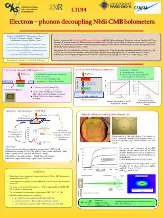
IR photons. ≈ 1 mm ≈ λ for IR absorption. IR photons. Electrons. I. NbSi film. e-ph coupling (weak at low T). 100 µm x 100 µm x 100 nm. Phonons. Cold bath = substrate. Kapitza coupling (strong). All electron bolometer. LTD14. Electron – phonon decoupling NbSi CMB bolometers.

Electron – phonon decoupling NbSi CMB bolometers
E N D
Presentation Transcript
IR photons ≈1 mm ≈λ for IR absorption IR photons Electrons I NbSi film e-ph coupling (weak at low T) 100 µm x 100 µm x 100 nm Phonons Cold bath = substrate Kapitza coupling (strong) All electron bolometer LTD14 Electron – phonon decoupling NbSi CMB bolometers Stefanos MARNIEROSa**, L.Dumoulina,C.Nonesa*,L.Bergéa, C.Marrache-Kikuchia , O.Rigauta, A.Monfardinib, A.Benoitb, Philippe Camusb aCSNSM, CNRS-IN2P3, Université Paris 11, Bat. 108, 91405 Orsay Campus, France b Institut Néel, CNRS/UJF, 25 rue des Martyrs, BP 166, 38042 Grenoble Cedex 9, France * Now at the Service de Physique des Particules - CEA/DSM/IRFU/SPP - 91191 Gif-sur-Yvette - France ** Email : Stefanos.Marnieros@csnsm.in2p3.fr In order to measure the Cosmological Microwave Background (CMB), high performance "bolometric cameras" similar to CCDs are currently developed worldwide. They are made out of thousands of pixels, each of which is a bolometer on its own. The goal is to increase the sensitivity by one or two orders of magnitude compared to the Planck satellite in order to meet the requirements for the CMB B-mode polarization observation. We propose here a new bolometer structure, allowing a simplification of the fabrication process and possibility to reach very low NEP. In this TES based detector, that can be either high (>1MW) or low (<1W) impedance, the three functions of a classical bolometer (wave absorption, temperature measurement and thermal decoupling) are achieved in a single NbxSi1-x film. Partially funded by ANR-06-BLAN-0326 and the CNES agency 1. Structure of usual CMB bolometers • Absorber (response time ∝volume) • Thermal sensor • Thermal decoupling through membranes → delicate fabrication IR photons Absorber Cold bath • Ultimate sensitivity limited by : • G=10-11 W.K-1 for Planck experiment (dependent on the membrane structure) • All use phonons as vectors for energy transport Sensor Thermal decoupling G Fast response time (independent of the film volume) Absorber = thermometer = NbSi TES 2. All electron bolometer alternative • Absorber= NbSi film • Thermal sensor = NbSi film • Thermal decoupling through NbSi electron-phonon decoupling Optical calibration with meander shaped TES TES Measurement of R → Heating due to incoming photons Absorption Square R meets vacuum impedance (377 Ω/□) → Maximum wave absorption 2mm Fabrication of a 204 pixel matrix. The sensors are NbxSi1-x TES with a meander shape deposited onto a 2” Si wafer. Different designs for the meanders have been tested. Weak e-ph coupling at low T Depends on T and • Advantages • Composition and thickness adjustable for operating T of 50-150 mK • Thermal decoupling: 10-9 W.K-1 for a film of 1 mm x 1 mm x 100 nm @ 70mK • Fast response time (≈ 1 ms @ 70 mK, 100µs @ 130mK) • Interdigited electrodes design → SQUID-based electronics • Meander-shaped NbSi design → JFET-based electronics The normal state resistance of the TES depends on the aspect ratio of the NbSi meander. In the present case it is adjusted to optimize performance with JFET input stage preamplifiers. Typical sensitivity dlog(R)/dlog(T) = 100 The TES behavior under higher bias is well described by the electron-phonon coupling model: P = ge-ph (Te5-Tph5) withge-ph = 200 W K-5 cm-3 • Conclusion • We measured direct absorption of infrared radiation by NbxSi1-x TES thermometers with an efficiency of 20%. • Electron-phonon decoupling inside the NbSi TES is used to replace the micromesh membranes. • The design can be used for low impedance (<1W) or high impedance (>1MW) TES. Can be adapted to multiplexing. • The performance of our detector is very promising: NEP= 2 10-16 W/√Hz • Substantial further progress can be achieved: • l/4 reflector to increase photon absorption efficiency • Lower T operation to decrease electron-phonon coupling • Use of antennas or lenses to reduce NbSi size (decrease Ge-ph) Measured light absorption coefficient: e = 20% Global performance (no excess noise observed): NEP= 2 10-16 W/√Hz