Download
1 / 26
290 likes | 751 Vues
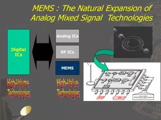
New Trends and Technologies for (N)MEMS Michael Kraft. Overview. Innovation sources for MEMS devices requirements for doing MEMS novel fabrication processes innovative design of micromachined structures system integration Key technologies for future MEMS devices

E N D
New Trends and Technologies for (N)MEMS Michael Kraft
Overview • Innovation sources for MEMS devices • requirements for doing MEMS • novel fabrication processes • innovative design of micromachined structures • system integration • Key technologies for future MEMS devices • Precision wafer bonding • Metrology and characterization • Conclusions
Requirements for ‘Doing’ MEMS A reasonable clean cleanroom Flexibility to introduce new materials Not having to worry about contamination Reasonable good lithography (~1um) Some special tools… Good metrology and measurement equipment • Southampton just opened a £80m facility with state of the art equipment
Southampton Nanofabrication Centre Micro • Flexible nanotechnology clean room • Silicon, glass, thin film technologies • 680m2 clean room (class 100 & 1000) • 110m2bioMEMS clean room (class 10000) • 110m2 thick film clean room (class 1000) • People • 14 academic staff • 6 clean room engineers • 50+ researchers • 50+ project students • … and many, many collaborators Carbon Nanotube bundles Si nanobridge with a single quantum dot cavity
Research Themes Lab-on-a-Chip Micro & Nano Electromechanical Systems Nanoelectronics Nanophotonics Quantum Information Technology Silicon Photovoltaics NEMS bridge as mechanical memory TEM sample preparation in a FIB
Innovation by Process Development MEMS has revolutionized sensors/actuators by making them small, low power, affordable through batch fabrication. Success stories include: pressure sensors, accelerometers, gyroscopes, flowsensors, etc. Past examples of process innovation: DRIE etching – the Bosch process. STS Pegasus DRIE etcher
New Process TechnologyExample: Ultra-smooth Optical Cavities Optical cavities can be used to detect single atoms Applications in quantum information technology Process technology challenge: cavities need to be ultra-smooth Optical fibre
Fabrication Process The silicon is etched using an ASE isotropic etch 3µm of Gold is sputtered The silicon nitride is stripped using orthophosphoric acid Photoresist is spun and patterned The resist is removed creating the finished chip A 50nm Chromium and 100nm Gold layer is sputtered 100nm of silicon nitride is deposited and patterned Photoresist is spun and patterned and the gold is ion beam milled The silicon is etched using a HF based solution A silicon substrate with 100nm of oxide deposited and patterned Silicon Innovation through novel combination of existing processes Chromium Photoresist Silicon oxide Gold Silicon nitride
Process Optimization Various etch rates can be used to make any radius of curvature Longer etch rates gives smoother mirrors Achieved around below 1nm rms roughness
Novel Design Approach for MEMS Example: Mechanical amplification • Most MEMS sensors rely on tiny deflections of a proof mass • The deflection is detected electronically by measuring a change in capacitance • Innovation: introduce a mechanical amplification stage • This is based on a simple leverage mechanism
Novel Design Approach for MEMS Example: Mechanical amplification
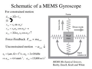
System Integration for MEMS Example: electromechanical control systems MEMS gyroscope (collaboration with Peking University) • Micromachined sensing element incorporated in an electromechanical sigma-delta modulator • This forms a force-feedback system with advantages over an open loop system • Better linearity, dynamic range, bandwidth, direct digital output
Bandpass SDM Interface for a MEMSGyro Spectra of simulated and measured results agree well Reduced sampling frequency compared to low-pass architecture SNR of 92dB with full scale input ‘Butterfly’ sensing element from SensoNor, Norway.
AtomChip: Multi domain integration Electrostatic xy comb drive Electrostatic z parallel plate Tuneable optical cavity Silicon Bose-Einstein atom cloud Fibre gold coated at the tip High current density gold wires
Atom Chips • Devices for trapping and manipulation of atoms on integrated microchips. • Quantum laboratories on chip. • Fundamental research • Quantum behaviour • Low dimensional physics • Entanglement and coupling • New devices – precise sensors • Atom interferometers • Atomic clocks • Accelerometers/Gyroscopes • Quantum information processing • Quantum computers
Overview • Innovation sources for MEMS devices • requirements for doing MEMS • novel fabrication processes • innovative design of micromachined structures • system integration • Key technologies for future MEMS devices • Precision wafer bonding • Metrology and characterization • Conclusions
Aligned Bonding for Multi Wafer MEMS EVG 520 bonder EVG 620 double sided mask aligner • Conventional approach: Aligner - bonder • For example from EVG • Accuracy ~1um
(Nano) Alignment Bonding 2.3mm SEM image of aligned and bonded chips. Vernier structures to evaluate bonding alignment IR image of a bonded sample ‘LEGO on a chip’ self-engaging alignment concept using cantilevers • Demonstrated 200nm alignment bonding at chip level • Only 10% of wafer area required for self-engaging structures • Wafer surface smooth enough for thermo-compression bonding
‘Repairing’ of N/MEMS: Focussed Ion Beam Zeiss NVISION40 FIB Machining of complex 3D structures Prototype post-processing
Characterization of MEMS • Polytec MSA400 MEMS dynamic tester • In plane and out of plane dynamic measurements • White light interferometer • 2D electrostatic actuator
Characterization of MEMS • Polytec MSA400 MEMS dynamic tester • In plane and out of plane dynamic measurements • White light interferometer • Investigation of levitation forces
High-res imaging: He Ion Microscope Orion image of CNTs 200nm bar • Description • Zeiss Orion He ion microscope • - Resolution <0.9nm • - High depth of focus • - High material contrast • - Rutherford backscattering analysis: • element identification • - Nanoengineering Orion image of CNTs 100nm bar Orion image of CNTs 50nm bar
Conclusions • Multi-functional MEMS is becoming mainstream • MEMS is in a transition to system-on-chip or system-in-a-package (micro-system-technology) • There are few really novel fabrication processes on the horizon • Rather new combinations of existing processes • There are still plenty of new design concepts to be explored • There are new characterization tools which are making an impact • The next BIG thing: • INTEGRATION INTEGRATION INTEGRATION