
Scalable Distributed Memory Machines: Massively Parallel Processors (MPPs) & Clusters
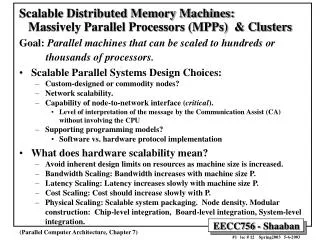
Scalable Distributed Memory Machines: Massively Parallel Processors (MPPs) & Clusters. Goal: Parallel machines that can be scaled to hundreds or thousands of processors. Scalable Parallel Systems Design Choices: Custom-designed or commodity nodes? Network scalability.

Scalable Distributed Memory Machines: Massively Parallel Processors (MPPs) & Clusters
E N D
Presentation Transcript
Scalable Distributed Memory Machines: Massively Parallel Processors (MPPs) & Clusters Goal: Parallel machines that can be scaled to hundreds or thousands of processors. • Scalable Parallel Systems Design Choices: • Custom-designed or commodity nodes? • Network scalability. • Capability of node-to-network interface (critical). • Level of interpretation of the message by the Communication Assist (CA) without involving the CPU • Supporting programming models? • Software vs. hardware protocol implementation • What does hardware scalability mean? • Avoid inherent design limits on resources as machine size is increased. • Bandwidth Scaling: Bandwidth increases with machine size P. • Latency Scaling: Latency increases slowly with machine size P. • Cost Scaling: Cost should increase slowly with P. • Physical Scaling: Scalable system packaging. Node density. Modular construction: Chip-level integration, Board-level integration, System-level integration. (Parallel Computer Architecture, Chapter 7)
Commodity Supercomputing:Cluster Computing • The research in heterogeneous supercomputing led to the development of high-speed system area networks and portable message passing environments. • These developments in conjunction with the impressive performance improvements and low cost of commercial general-purpose microprocessors led to the current trend in high-performance parallel computing of moving away from expensive specialized traditional supercomputing platforms to cluster computing that utilizes cheaper, general purpose systems consisting of loosely coupled commodity of-the-shelf (COTS) • Such clusters are commonly known as Beowulf clusters and are comprised of three components: • Computing Nodes: Each low-cost computing node is usually a small Symmetric Multi-Processor (SMP) system that utilizes COTS components including commercial General-Purpose Processors (GPPs) with no custom components. • System Interconnect: Utilize COTS Ethernet-based or system area interconnects including Myrinet and Dolphin SCI interconnects originally developed for HSC. • System Software and Programming Environments: Such clusters usually run an open-source royalty-free version of UNIX (Linux being the de-facto standard). The message-passing environments (PVM , MPI), developed originally for heterogeneous supercomputing systems, provide portable message-passing communication primitives. From Lecture 6
Communication Assist: MPPs: Custom Clusters: COTS Message-Passing Parallel Systems:Commercial Massively Parallel Processor Systems (MPPs) Vs. Clusters Parallel Programming: Between nodes: Message passing using PVM, MPI In SMP nodes: SAS Multithreading using Pthreads, OpenMP Operating system? MPPs: Proprietary Clusters: royalty-free (Linux) MPPs vs. Clusters • MPPs: “Big Iron” machines • COTS components usually limited to using commercial processors. • High system cost • Clusters: Commodity Supercomputing • COTS components used for all system components. • Lower cost than MPP solutions • Scalable Network: • Low latency • High bandwidth • MPPs: Custom • Clusters: COTS • Gigabit Ethernet • System Area Networks (SANS) • ATM • Myrinet • SCI S c a l a b l e n e t w o r k Distributed Memory S w i t c h S w i t c h S w i t c h ° ° ° C A M $ P Node: O(10) SMP MPPs: Custom node Clusters: COTS node (workstations or PCs) Custom-designed CPU? MPPs: Custom or commodity Clusters: commodity From Lecture 6
MPPs Scalability Issues • Problems: • Total available bandwidth. • Memory-access latency (local vs. remote access). • Interprocess communication complexity or synchronization overhead. • Multi-cache inconsistency. • Message-passing and message processing overheads. • Possible Solutions: • Fast dedicated, proprietary and scalable, networks and protocols. • Low-latency fast synchronization techniques possibly hardware-assisted . • Hardware-assisted message processing in communication assists (node-to-network interfaces). • Weaker memory consistency models. • Scalable directory-based cache coherence protocols (Next lecture, PCA ch. 8) • Shared virtual memory implemented with hardware support. • Improved software portability: standard parallel programming environments and operating system support. • Software latency-hiding techniques.
Poor Scalability One Extreme:Limited Scaling of SMPs Using a Bus • Bus-Based SMPs: Each level of the system design is grounded in the scaling limits at the layers below and assumptions of close coupling between components. Characteristic Bus Physical Length ~ 1 ft Number of Connections fixed Maximum Bandwidth fixed Interface to Comm. medium memory interface + coherence protocols Global Order arbitration Protection Virt -> physical Trust total OS single comm. abstraction HW - Limited Concurrent transactions - Globally ordered transactions via arbitration. - Limited fixed bandwidth.
Another Extreme:Scaling of Clusters of Workstations Using a LAN? • No clear limit to physical scaling, no global order. • Usually high communication latency. • System Area Networks (SANS): Alternative Networks for clusters • Scalable, high bandwidth, low latency and protocol overheads. • Myrinet, SCI, ServerNet … ATM 622 mb/s FDDI 100 mb/s Switch-based Fast/Gigabit Ethernet SANS Myrinet 2 Gb/s Characteristic Bus LAN Physical Length ~ 1 ft KM Number of Connections fixed many Maximum Bandwidth fixed ??? Interface to Comm. medium memory inf peripheral Global Order arbitration ??? Protection Virt -> physical OS Trust total none OS single independent comm. abstraction HW SW
Bandwidth Scalability Scalable Parallel Machine • Bandwidth scalability depends largely on network characteristics: • Channel bandwidth. • Static: Topology: Node degree, Bisection width etc. • Multistage: Switch size and connection pattern properties. • Node-to-network interface (Communication Assist CA) capabilities.
Dancehall MP Organization • Network bandwidth? • Bandwidth demand? • Independent processes? • Communicating processes? • Network bandwidth requirement scale linearly with P • Latency? MIN Extremely high demands on network in terms of bandwidth, latency even for independent processes.
Communication Assist Extent of functionality? DMA, user-level access user-level handlers Generic Distributed Memory Organization OS Supported? Network protocols? • Network bandwidth? • Bandwidth demand? • Independent processes? • Communicating processes? • Latency? O(log2P) increase? • Cost scalability of system? Multi-stage interconnection network (MIN)? Point-to-point? Custom-designed? SAN? Global physical or virtual Shared address space support? Message transaction DMA? Node: O(10) Bus-based SMP Custom-designed CPU? Node/System integration level? How far? Cray-on-a-Chip? SMP-on-a-Chip?
Key System Scaling Property • Bandwidth should increase with P, while latency remains low. • Large number of independent communication paths between nodes. => Allow a large number of concurrent transactions using different channels. • Transactions are initiated independently. • No global arbitration. • Effect of a transaction only visible to the nodes involved • Effects propagated through additional transactions.
Network Latency Scaling • T(n) = Overhead + Channel Time + Routing Delay • Scaling of overhead? f(n)? • Channel Time(n) = n/B --- BW at bottleneck • RoutingDelay(h,n) = h D Assuming cut-through routing is used
Only 20% increase in latency for 16x size increase ~ 60% increase in latency for 16x size increase Network Latency Scaling Example O(log2 n) Stage MIN using switches: • Max distance: log2 n • Number of switches: a n log n • overhead = 1 us, BW = 64 MB/s, D = 200 ns per hop • Using pipelined or cut-through routing: • T64(128) = 1.0 us + 2.0 us + 6 hops * 0.2 us/hop = 4.2 us • T1024(128) = 1.0 us + 2.0 us + 10 hops * 0.2 us/hop = 5.0 us • Store and Forward • T64sf(128) = 1.0 us + 6 hops * (2.0 + 0.2) us/hop = 14.2 us • T1024sf(128) = 1.0 us + 10 hops * (2.0 + 0.2) us/hop = 23 us
Cost Scaling • cost(p,m) = fixed cost + incremental cost (p,m) + Network(p) • Bus Based SMP? Fixed-cost high • Ratio of processors : memory : network : I/O ? • Parallel efficiency(p) = Speedup(P) / P • Similar to speedup, one can define: Costup(p) = Cost(p) / Cost(1) • Cost-effective: speedup(p) > costup(p) memory
Cost Effective? 2048 processors: 475 fold speedup at 206x cost Using MINs?
Parallel Machine Network Examples SAN: 8x8 switches 2Gb/s
Physical Scaling Physical node construction, density/integration • Chip-level integration: • Integrate network interface, message router I/O links. • nCUBE/2, Alpha 21364, IBM Power 4, AMD Opetron • IRAM-style Cray-on-a-Chip: V-IRAM • Memory/Bus controller/chip set: Alpha 21364, AMD Opetron • SMP on a chip: Chip Multiprocessor (CMP): IBM Power 4 • Board-level integration: • Replicating using standard microprocessor cores. • CM-5 replicated the core of a Sun SparkStation 1 workstation. • Cray T3D and T3E replicated the core of a DEC Alpha workstation + custom shell logic + CA. • System level integration: • IBM SP-2 uses 8-16 almost complete RS6000 workstations placed in racks + custom CA, network, system software.
B a s i c m o d u l e D R A M i n t e r f a c e s l r e e A M M U n t u M n o a D R h I - F e t c h c O p e r a n d H y p e r c u b e n e t w o r k & $ c o n f i g u r a t i o n d e c o d e S i n g l e - c h i p n o d e E x e c u t i o n u n i t 6 4 - b i t i n t e g e r I E E E f l o a t i n g p o i n t Chip-level integration Example:nCUBE/2 Machine Organization • Entire machine synchronous at 40 MHz (25ns) • Routing delay = 2.2 usec 64 nodes socketed on a board Memory Interface Reduced VAX 13 bit-serial links up to 8096 nodes possible (2048 built) 500, 000 transistors (considered large at the time,1991)
8 x 64 or 16 x 32 or 32 x 16 + 2-way Superscalar x Vector Instruction ÷ Processor Queue I/O Load/Store I/O Vector Registers 8K I cache 8K D cache 8 x 64 8 x 64 Memory Crossbar Switch M M M M M M M M M M … M M M M M M M M M M 8 x 64 8 x 64 8 x 64 8 x 64 8 x 64 I/O … … … … … … … … … … I/O M M M M M M M M M M Chip-level integration Example:Vector Intelligent RAM 2 (V-IRAM-2) Projected 2004. < 0.1 µm, > 2 GHz 16 GFLOPS(64b)/64 GOPS(16b)/128MB
Address In R A M B U S 21264 Core 16 L1 Miss Buffers Memory Controller Address Out Network Interface 64K Icache L2 Cache North South East WestI/O 64K Dcache 16 L1 Victim Buf 16 L2 Victim Buf Chip-level integration Example:Alpha 21364 • Alpha 21264 core with enhancements • Integrated Direct RAMbus memory controller: • 800 MHz operation, 30ns CAS latency pin to pin, 6 GB/sec read or write bandwidth • Directory based cache coherence • Integrated network interface: • Direct processor-to-processor interconnect, 10 GB/second per processor • 15ns processor-to-processor latency, Out-of-order network with adaptive routing • Asynchronous clocking between processors, 3 GB/second I/O interface per processor
IO M IO M M IO M M IO IO IO M IO M IO M IO M IO M IO M IO M 364 364 364 364 364 364 364 364 364 364 364 364 Chip-level integration Example:A Possible Alpha 21364 System
Chip-level integration Example: IBM Power 4 CMP • Two tightly-integrated > 1GHz CPU cores per 170 Million Transistor chip. • 128KB L1 Cache per processor • 1.5 MB On-Chip Shared L2 Cache • External 32MB L3 Cache: Tags kept on chip. • 35 Gbytes/s Chip-to-Chip interconnects.
Chip-level integration Example: IBM Power 4
Chip-level integration Example: IBM Power 4 MCM
Board-level integration Example:CM-5 Machine Organization (1993) Fat Tree 33 MHz SPARC Design replicated the core of a Sun SparkStation 1 workstation Other Board-level Integration Examples: Cray T3D, T3E (Alpha processors), Intel ASCI Red (Pentium Pro), Intel Paragon (i860) ….
System Level Integration Example: IBM SP-1/SP-2 8-16 almost complete RS6000 workstations placed in racks. MIN Also IBM ASCI White (Power3) 40 MB/s
CAD Database Scientific modeling Parallel applications Multipr ogramming Shar ed Message Data Pr ogramming models addr ess passing parallel Compilation Communication abstraction or library User/system boundary Operating systems support Har dwar e/softwar e boundary Communication har dwar e Physical communication medium Realizing Programming Models:Realized by Protocols Network Transactions
Challenges in Realizing Prog. Models in Large-Scale Machines • No global knowledge, nor global control. • Barriers, scans, reduce, global-OR give fuzzy global state. • Very large number of concurrent transactions. • Management of input buffer resources: • Many sources can issue a request and over-commit destination before any see the effect. • Latency is large enough that one is tempted to “take risks”: • Optimistic protocols. • Large transfers. • Dynamic allocation. • Many more degrees of freedom in design and engineering of these system.
Scalable Network Message Input Processing – checks – translation – buffering – action Output Processing – checks – translation – formating – scheduling ° ° ° CA Communication Assist CA Node Architecture M P M P Network Transaction Processing Key Design Issue: • How much interpretation of the message by CA without involving the CPU? • How much dedicated processing in the CA? CA = Communication Assist
Extent of CA Interpretation of Network Transactions: Spectrum of Designs 1 None: Physical bit stream • blind, physical DMA nCUBE, iPSC, . . . 2 User/System • User-level port CM-5, *T • User-level handler J-Machine, Monsoon, . . . 3 Remote virtual address • Processing, translation Paragon, Meiko CS-2 4 Global physical/virtual address • Proc + Memory controller RP3, BBN, T3D, T3E 5 Cache-to-cache • Cache controller Dash, KSR, Flash Increasing HW Support, Specialization, Intrusiveness, Performance (???)
sender auth Copy DMA User Area Kernel Area Network dest addr DMA Copy Network Kernel Area User Area 1 No CA Net Transactions Interpretation: Physical DMA • DMA controlled by registers, generates interrupts. • Physical => OS initiates transfers. • The destination processor initiates a DMA transfer from the network • The next incoming network message is blindly stored in system buffer. • Send-side: • Construct system “envelope” around user data in kernel area. • Receive: • Must receive into system buffer, since no message interpretation in CA. System-Level Network Ports
1 Blind DMA Example: nCUBE/2 Network Interface • Independent DMA channel per link direction • Leave input buffers always open. • Segmented messages. • Routing determines if message is intended for local or remote node • Dimension-order routing on hypercube. • Bit-serial with 36 bit cut-through. Os Send 16 ins 260 cy 13 us OS Receive 18 ins 200 cy 15 us - includes interrupt 150 us message-passing library overhead
Host Memory NIC trncv Data NIC Controller addr Addr Len Status Next Addr Len Status Next Addr Len Status Next Addr Len Status Next Addr Len Status Next Addr Len Status Next TX DMA RX len IO Bus mem bus Proc DMA In Conventional LAN Network Interfaces Receive DMA Descriptors Send DMA Descriptors DMA Input/ Output Queues Fast Ethernet, ATM ...
CA CA 2 User-Level Network Ports • Initiate transaction at user level. • CA interprets and delivers message to user without OS intervention. • Network port in user virtual address space. • User/system flag in envelope. • Protection check, translation, routing, media access in source CA • User/sys check in destination CA, interrupt on system. Appear to user as logical message queues plus status
2 User-Level Network Example: CM-5 • Two data networks and one control network. • Input and output FIFO for each network. • Tag per message: • Index Network Inteface (NI) mapping table. • *T integrated NI on chip. • Also used in iWARP. • Five-word Message Os 50 cy 1.5 us Or 53 cy 1.6 us interrupt 10us Latency 3-5 us To user level
U s e r / s y s t e m D a t a A d d r e s s D e s t ° ° ° M e m M e m P P 2 User-Level Handlers • Tighter integration of user-level network port with the processor at the register level. • CA is essentially a function unit in the processor. • Hardware support to vector to address specified in message • Network message ports in processor registers. • Greatly reduced latency: Data moved in and out of network using register-to-register instructions.
Host Interface unit 2 User-Level Handlers Example iWARP • Nodes integrate communication with computation on systolic basis. • Message data direct to register (word by word) Or • Stream into memory (DMA). Two registers are bound to network input/output ports
Network dest ° ° ° Mem Mem NI NI P P M P M P User System User System 3 Remote/Global Virtual Address SpaceDedicated Message Processing Without Specialized Hardware Design One of the SMP node processors serves as a dedicated communication (CP) or message processor (MP) that handles network transaction processing, message interpretation and possibly global address operations in software. Message processor performs arbitrary output processing (at system level) Message processor interprets incoming network transactions (at system level) User Processor <–> Message Processor share memory Message Processor <–> Message Processor via system network transaction MP Message Processor Node: Bus-based SMP
Network dest ° ° ° Mem Mem NI NI M P M P P P User System Levels of Network Transaction • User Processor stores cmd / msg / data into shared output queue. • Communication assists make transaction happen. • Checking, translation, scheduling, transport, interpretation. • Effect observed on destination address space and/or events. • Reduces overhead on user processor but adds latency Node: Bus-based SMP MP Message Processor MP can also be integrated in NI
Example: Intel Paragon (1992) Service Network I/O Nodes I/O Nodes Devices Devices 16 175 MB/s Duplex rte MP handler Mem 2048 B ° ° ° EOP Var data NI 64 i860xp 50 MHz 16 KB $ 4-way 32B Block MESI 400 MB/s sDMA $ $ rDMA P M P
4 Global Virtual/Physical Address Space Using Specialized Hardware Design • Shared physical/virtual address space realized with specialized hardware to provide global loads, stores, and atomic memory operations. • The specialized communication assist is viewed as a pseudo-memory module and pseudo-processor that translates bus transactions into network transactions. • The memory management unit (MMU) translates a virtual address into a global physical address presented to the memory system. • If the global physical address is local the local memory responds, if not the CA acts as a memory module while accessing the remote location by extracting remote node number from the physical address and issuing a network transaction. • The remote CA acts as pseudo-processor to its node by reading the desired memory location and then issues a network transaction in response. • Early designs used the dancehall organization while later designs used distributed memory. • Examples include: CM*, NYU Ultracomputer, BBN Butterfly, IBM RP3, Denelcor HEP-1, BBN TC200 and Cray T3D, T3E
4 Global Virtual/Physical Address Space ExampleCray T3E Overview of the Cray T3E: • Self-hosted running Unicos/mk. • Logically shared address space over physically distributed memory (up to 2 GB per processor). • Each PE contains: • A DEC Alpha 21164 CPU (initially at 300 MHz ) • Shell logic: control chip, router chip, local memory (75MHz) • External 64-bit registers (E-registers): 512 user 128 system, used for all remote communication and synchronization. • Up to 2048 are connected by a 3D torus with fully adaptive minimal routing. • No board-level cache; only internal CPU cache (8K L1, 96K L2). • Only local memory is cached; cache coherency through the use of external backmap to probe and update on-chip cache. • Network links: Time multiplexed; one 64-bit word each 13.3 ns (five times faster than system clock). • GigaRing channel I/O: 267 MB/s sustained for every four processors.
T3E Processing Element (PE) Block Diagram Control & External E-Registers
T3E Global Communication • E-registers: • Extend the physical address space of the CPU. • Increase degree of pipelining for global memory requests. • Direct loads and stores performed between E-registers and CPU. • Global E-register operations used for global data transfer (local or remote), messaging, and atomic-operation synchronization. • Global E-register operations use a global virtual address formed by shell logic: • Virtual PE address translated to physical PE at the source. • Virtual address transmitted across the net is translated to a physical address using a global translation buffer at the target PE • Data distribution features of many implicit programming languages (i.e broadcast/gather/scatter) supported using an integrated hardware centrifuge.
Remote Data Access Using E-Registers • Loading remote data into an E-register involves three steps: • The processor portion of the global virtual address is constructed in an address E-register • A get command is issued via a store to a special region in memory that specifies the destination E-register • Get command sets the destination E-register to empty • Causes the remote read to be performed and the destination E-register to be loaded with the data and set to full when the get completes. • Finally the data is read into the processor via a load from the data E-register • If the processor attempts to load from an empty E-register, the memory operation is stalled until the get completes. • The process for a remote put is similar, except the store data is placed in the data E-register specified in the put command while another address E-register has global virtual address.
T3E Barrier/Eureka Synchronization • Barriers allow a set of participating processors to determine when all processors have signaled some event • Eurekas allow a set of processors to determine when any one of the processors has signaled some event. • The T3E provides a set of 32 barrier/eureka synchronization units (BSUs) at each processor. • The BSUs are accessible as memory-mapped registers and are allocated and protected via the address translation mechanism. • A set of processors can be given access to a particular BSU through which they can perform barrier and/or eureka synchronization. • Multiple disjoint sets of processors may reuse the same logical BSU. • A BSU at a processor can be in one of several states. • Processors can read this state and perform operations on the BSU via load and store operations.