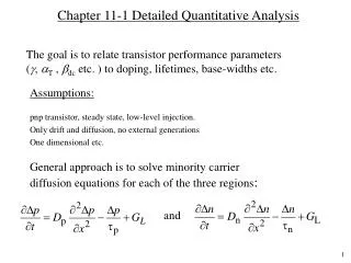
Chapter 11-1 Detailed Quantitative Analysis
Chapter 11-1 Detailed Quantitative Analysis. The goal is to relate transistor performance parameters ( , T , dc etc. ) to doping, lifetimes, base-widths etc. pnp transistor, steady state, low-level injection. Only drift and diffusion, no external generations One dimensional etc.

Chapter 11-1 Detailed Quantitative Analysis
E N D
Presentation Transcript
Chapter 11-1 Detailed Quantitative Analysis The goal is to relate transistor performance parameters (, T , dc etc. ) to doping, lifetimes, base-widths etc. • pnp transistor, steady state, low-level injection. • Only drift and diffusion, no external generations • One dimensional etc. Assumptions: General approach is to solve minority carrier diffusion equations for each of the three regions: and
General Quantitative Analysis Under steady state and when GL= 0, and For the base in pnp, we are interested only in holes. we are going to take a simplified approach.
Injection Efficiency : Base transport factor :aT =IC / IEP Collector to emitter current gain: aDC =aT g Collector to base current gain: bDC =aDC / (1 – aDC) Review: Operational Parameters IEP IBR –IEN –IBE –IBR
Review of P-N Junction Under Forward Bias + VEB nE(0) pB(0) P (emitter) N (base) Area = Qp Area = Qn pB0 nE0 xE xB 0 0
Review of P-N Junction Under Forward Bias (cont.) In = q A DE dn/dxE = – (q A DE/LE) nE(0) Ip= – q A DB dp/dxB = (q A DB/LB) pB(0) Total current I = IP +(– IN) (“–” because xE and xB point in opposite directions) = (q A DB/LB) pB(0) + (q A DE/LE) n E (0) = (q A DB/LB) pB0[exp (q VEB / kT) –1] + + (q A DE/LE) nE0[exp (q VEB /kT) –1] ≈(q A DB/LB) pB0 exp (q VEB/kT) + (q A DE/LE) nE0 exp (q VEB/kT) Note ! Ip and In can also be calculated based on the fact that Qp has to be replaced every B seconds Ip = Qp/B and In = Qn/E and IE = IP + IN
Emitter Base Collector pB(0) nE(0) nC0 pB0 nE0 nC(0) Simplified Analysis Consider the carrier distribution in a forward active pnp transistor
Simplified Analysis (cont.) nE0, pB0 and nC0 = equilibrium concentration of minority carriers in emitter, base and collector nE(0), pB(0)and nC(0) = minority carrier concentration under forward active conditions at the edge of the respective depletion layers nE (0), pB(0)and nC(0) = Excess carrier concentration at the edge of the depletion layers
Simplified Analysis (cont.) nE (0) = nE (0) – nE0 = nE0 [exp (q VEB / kT) – 1] pB (0) = pB (0) – pB0 = pB0 [exp (q VEB / kT) – 1] By taking the slopes of these minority carrier distribution at the depletion layer edges and multiplying it by “qAD”, we can get hole and electron currents. Note that In = q A Dn (dn/dx) and Ip = – q A Dp (dp / dx)
Calculation of Currents • Collector current, IC • Ic = q A DB (dp/dxB) (slope must be taken at end of base) • = q A DB [pB(0) – 0] / WB • = q A DB pB(0) / WB • Ic = q A (DB/WB) pB0 exp (qVEB / kT)---- (A) • (only hole current if we neglect the small reverse saturation current of reverse biased C-B junction)
Calculation of Currents (cont.) • Emitter Current, IE • IE is made up of two components, namely IEP and IEN • IEP = Ic + current lost in base due to recombination • = Ic + excess charge stored in base/B • = Ic + q A WBpB(0) / (2B) • q A (D B/W B) pB0 [exp (qVEB / kT) ] • + q A [W B/(2B)] pB0 [exp (qVEB / kT)] --- (B) • [ Assuming exp (qVEB / kT) – 1 exp (qVEB / kT) • when VEB is positive, i.e forward biased. ]
Calculation of Currents (cont.) • Emitter Current (cont.) • IEN corresponds to electron current injection from base to emitter since E-B junction is forward biased. • IEN = qA (D E / LE) nE0 [exp (q VEB / kT) – 1 ] • qA (D E / LE) nE0 [exp (q VEB / kT)] ----- (C)
Calculation of Currents (cont.) • Base Current, IB • supplies electrons for recombination in base • supplies electrons for injection to emitter. • IB = qA pB0 [WB / (2B )] [exp (qV EB / kT) ] • + • qA(D E / LE) nE0 exp (qV EB / kT) • ( recombination) + (electron injection to emitter) • Now we can find transistor parameter easily.
Calculation of Currents (cont.) Base transport factor, T T = IC / IEP (same as eq. 11.42 in text) Emitter injection efficiency, = IEP / [ IEP + IEN ] = 1 / [ 1 + IEN / IEP ] = 1 / [ 1+ (C) / (B)]
DC = DC / (1– DC ) Calculation of Currents (cont.) nE0 = ni2/ NE … doping in emitter pB0 = ni2/ NB … doping in base dc= T