Download
1 / 25
260 likes | 501 Vues
SEU Hardened Clock Regeneration Circuits. By: Rajballav Dash Rajesh Garg Sunil P. Khatri Gwan Choi Department of Electrical and Computer Engineering, Texas A&M University, College Station, TX. Outline. Background Motivation Previous Work Our Approach Experimental Results

E N D
SEU Hardened Clock Regeneration Circuits By: Rajballav Dash Rajesh Garg Sunil P. Khatri GwanChoi Department of Electrical and Computer Engineering, Texas A&M University, College Station, TX
Outline • Background • Motivation • Previous Work • Our Approach • Experimental Results • Conclusions
Charge Deposition by a Radiation Particle • Radiation particles - protons, neutrons, alpha particles and heavy ions • Reverse biased p-n junctions are most sensitive to particle strikes • Charge is collected at the drain nodethrough drift and diffusion • Results in a voltage glitch at the drain node • System state may change if this voltage glitch is captured by at least one memory element • This is called SEU • May cause system failure Radiation Particle VDD G S D _ + n+ n+ Depletion Region + _ + _ E _ + _ E + VDD - Vjn _ + _ + _ + p-substrate B
Radiation Strike Model • Charge deposited (Q) at a node is given by where: Lis the Linear Energy Transfer (MeV-cm2/mg) t is the depth of the collection volume (mm) • A radiation particle strike is modeled by a current pulse as where: : Qcoll is the amount of charge collected (assumed Qcoll = QD in worst case analysis) tais the collection time constant tb is the ion track establishment constant • The radiation induced current always flows from n-diffusion to p-diffusion
Motivation • Modern VLSI Designs • Vulnerable to noise effects- crosstalk, SEU, etc • Single Event Upsets (SEUs) or Soft Errors • Troublesome for both memories and combinational logic • Need to efficiently design radiation tolerant circuits for critical applications • Clock node upsets are also becoming problematic • SEUs due to radiation particle strikes on clock nodes • Accounts for nearly 20% of the overall sequential soft error rate (SER) – Seifert et al. 2005
Clock Distribution Networks • Global clock distribution network • Immune to radiation particle strikes • Negligible contribution (0.1%) to overall SER • Large clock buffers and large node capacitances • Smaller active area compared to regional clock regenerators • Regional clock regenerators (RCG) • Susceptible to radiation particle strikes • Drive small load at its output • Clock inverter are progressively sized • Radiation strikes can results in radiation-induced race and radiation-induced clock jitter • The focus of this talk is to present radiation tolerant regional clock regenerator designs
Previous Work • Very few research efforts have addressed the issue of clock node upsets • Seifert et al. 2005 analyzed the effect of clock node upsets • Clock node strikes contributes ~20% to total sequential SER • Radiation-induced jitter contributes less than 2% of total sequential SER • Upsets in the local regenerator circuit contributed significantly to the overall sequential SER • Katz et al. 1998 performed experimental analysis to estimate the contribution of clock node upset to chip level SER on a “RH1020” chip • Clock upset rate has strong and linear dependence on clock frequency • Ad-hoc methods like reducing clock frequency and redundancy were discussed qualitatively – no results were presented
Our Approach • Part 1 –Analyze the effect of radiation particle strike on a regular regional clock regenerator (RCG) circuit • We propose 2 hardening approaches for regional clock regenerators • Part 2 –Triple modulo redundancy (TMR) based radiation hardening • Part 3 –Our split-output inverter based radiation hardening approach
Regular Unhardened RCG • GCLK: Clock from global clock distribution grid • RCLK:Clock input to the sequential load • CL:a128X Inverter (Typically a RCG drives a load of around 64 master-slave D flip- flops) • NAND gate and inverters are progressively sized with a staging ratio of ~3 • Simulated a radiation particle strike at n1 corresponding to Q = 150fC, ta = 150ps and tb = 38ps • Results in radiation-induced raceand radiation-induced jitter at RCLK – Worst case pulse width is 442ps and jitter is 833ps
TMR based Hardened RCG • Three parallel regenerator circuits are used • Three parallel signals are fed to the majority function (MF) • MF implements voting logic to generate correct signal at n3 • Voting logic function is • MF is sized up to 15X to protect RCLK from radiation strikes at n3 • RCLK is immune to radiation strikes at output of B4 for Q ≤ 150fC • Clock regenerator is tolerant to radiation particle strikes
in Radiation Tolerant Split-output Inverter (Garg et al. 2008) • A radiation particle strike at a reverse biased p-n junction results in a current flow from n-type diffusion to p-type diffusion inp out1p inp & inn Radiation Particle VDD - VTN out2 out1n out2 out1p |VTP| out1 out2 INV1 INV2 out1n inn Radiation Particle Modified Inverter Radiation Tolerant Inverter INV2 INV1
Radiation Tolerant Split-output Inverter (Garg et al. 2008) Radiation Particle Strike inp X Radiation Particle Strike M8 M2 X inp & inn out1p X M4 X M6 out1n out2 out1p X M5 out2 M3 The voltage at out2 is unaffected out1n A radiation particle strike at any node of the first inverter (radiation tolerant inverter) does not affect the voltage at out2 X M7 M1 inn
First Step: Split-output based RCG Hardening • A simple solution would be to replace gates B1, B2 and B3 by their hardenedcounterparts obtained using split-output inverter • This solution will not be 100% tolerant to radiation particle strikes • Assume a radiation strike at out1p just after bothout1p and out1n had fallen to GND and before out2 has risen to VDD • out2 enters high impedance state with GNDor some intermediate voltage – wrong state • This may delay a clock edge at RCLK resultingin a large clock jitter inp M8 out1p out2 out1n inn M7 INV2 INV1
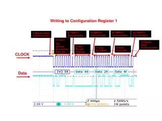
Second Step: Split-output based RCG Hardening • Duplicate gates B1, B2, B3 and B4 and replace them by their hardened counterparts • Output of B4 are op and on - op (on) is driven by only PMOS (NMOS) • op (on) can only experience 0 to 1 (1 to 0) flip due to a strike at op (on) • Similarly, B4d gates has opd and ond outputs • Generate correct clock signal using op, on, opd and ond signals • Using Karnaugh map, we obtain RCLK = op.opd • This design is still not tolerant to radiation particle strikes • 1 to 0 flip possible on opdue to a particle strike at n3_1p Radiation Particle Strike
Final Design: Split-output based RCG Hardening • We need to ensure that op and opddo not experience 1 to 0 flip due to a particle strike anywhere in RCG • Only0 to 1 flip is allowed on op and opd • Both inputs of B4 (B4d) are driven by n3_1n (n3_2n) • A particle strike at n3_1n and n3_2n can result in only 1 to 0 flip at inputs of B4 and B4d – ensures only 0 to 1 flip occur at op and opd • Inputs of B3 (B3d) are n2_1p (n2_2p) which can experience 0 to 1 flip • Repeat this process until we reach the outputs of B1 and B1d • The resulting RCG design is tolerant to radiation particle strikes
Experimental Setup • We implemented unhardened and hardened regional clock regenerators (RCG) • Using a 65nm PTM model card with VDD = 1.0V • We simulated radiation particle strikes • Q=150fC, ta=150ps & tb=38ps • At all the nodes of the two clock regenerator circuits • At different times during the clock period • Clock frequency is assumed to be 2 GHz • Layouts were created for all RCGs using Cadence SEDSM
Experimental Results • Comparison of radiation tolerance of regular unhardened, TMR based and split-output inverter based hardened RCGs • All measurements are made at RCLK • In the worst case, a radiation strike at regular RCG may completely eliminate a clock pulse • Radiation-induced jitter is also large for regular RCG • Both TMR and our split-output based approaches eliminate radiation-induced voltage glitches • Split-output inverter based approach is more effective in reducing radiation-induced jitter than the TMR based approach • Rise/fall times of both hardening approaches are comparable
Performance Comparison of Our Hardening Approaches • TMR based radiation hardened RCG consumes more dynamic power and require more layout area than the split-output inverter based radiation hardened RCG • Leakage current is slightly higherfor the split-output based RCG than the regular and TMR based RCGs
Conclusions • Radiation strikes in clock nodes in regional clock regenerators contribute to ~20% of overall chip level SER • We developed two techniques to harden regional clock regenerators • TMR based approach • Split-output inverter based approach • Our both approaches are very effective • Completely eliminate radiation-induced race • Suppress radiation-induced jitter to low values 58ps and 30ps • Critical charge is ~150fC • The split-output inverter based has a slight advantage over TMR based approach • Consumes lower dynamic power and require lower area • However, TMR based approach exhibits lower leakage
in Radiation Tolerant Split-output Inverter (Garg et al. 2008) • A radiation particle strike at a reverse biased p-n junction results in a current flow from n-type diffusion to p-type diffusion • A gate constructed using only PMOS (NMOS) transistors cannot experience 1 to 0 (0 to 1) upset Radiation Particle inp out1p inp & inn VDD - VTN out2 out2 out1 out1n out1p |VTP| INV1 INV2 out1n Radiation Particle inn out2 INV2 INV1 Static Leakage Paths
inp & inn VDD - VTN out1n out1p |VTP| out2 Radiation Tolerant Split-output Inverter Low VT transistors inp inp out1p out1p X out2 out2 out1n X inn out1n Leakage currents are lower by ~100X inn Radiation Tolerant Inverter Modified Inverter
First Step: Split-output based RCG Hardening • A simple solution would be to replace all the gates in the circuit with hardened split-output gates as shown alongside • Problems with this design: • For hardened gates, radiation strike at any output node takes next inverter output to high impedance as shown in previously. • This causes delay in clock edge at R_CLK node • Large Clock Jitter • This problem is dealt in the next step by duplicating the hardened inverter chain and then masking the delay-difference
Second Step: Design using Split-Output Gates and Masking Function • Hardens nodes op, on, opd, ond, n5 and R_CLK only • Problems with this design: • Radiation strike at any other node (e.g. n3_1n) may result in 1->0 (0 ->1) transition at op/opd (on/ond) (e.g. op) nodes as shown figure which is considered don’t care condition in the k-map • This problem is dealt in the next step by limiting the transition to only one type at the input of the hardened gates so that only one transition is seen at op and opd.
Final Design: Split-Output Inverter based Clock Regenerator Circuit • Advantage: • Radiation Strike can cause only one transition at the input of each hardened gate for which only one transition can occur at n4_1p and n4_2p due to radiation strike which is rejected by the masking AND gate (B5). • Note: In practice, the 2X inverter can directly drive the 8X inverter. An extra stage was added for demonstrating the working principle of the circuit in a generic sense.