Download
1 / 19
190 likes | 236 Vues
Explore advanced test methods for VLSI devices operating at high clock rates, addressing testing challenges, timing methods, voltage testing, delay testing, slow-clock testing, and BIST techniques.

E N D
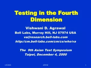
Testing in the Fourth Dimension Vishwani D. Agrawal Bell Labs, Murray Hill, NJ 07974 USA va@research.bell-labs.com http://cm.bell-labs.com/cm/cs/who/va The 9th Asian Test Symposium Taipei, December 4, 2000 ATS'00
Present and Future* 1997 -2001 2003 - 2006 Feature size (micron) 0.25 - 0.15 0.13 - 0.10 Transistors/sq. cm 4 - 10M 18 - 39M Pin count 100 - 900 160 - 1475 Clock rate (MHz) 200 - 730 530 - 1100 Power (Watts) 1.2 - 61 2 - 96 * SIA Roadmap, IEEE Spectrum, July 1999 ATS'00
Cost of Testing in 2000AD • 0.5-1.0GHz, analog instruments,1,024 digital pins: ATE purchase price • = $1.2M + 1,024 x $3,000 = $4.272M • Running cost (five-year linear depreciation) • = Depreciation + Maintenance + Operation • = $0.854M + $0.085M + $0.5M • = $1.439M/yr • Test cost (24 hour ATE operation) • = $1.439M/(365 x 24 x 3,600) • = 4.5 cents/second ATS'00
Challenges of Testing • High-speed tests for transition faults or critical paths are useless unless tests are applied by the ATE at the rated clock speed • Too expensive to replace current ATE with high-speed ATE • Non-availability of high-speed ATE and lack of compatibility among ATE manufacturers • Speed gap between VLSI speed and ATE speed may always exist • Noise problems (coupling, mismatch, etc.) in high-speed ATE to DUT interface ATS'00
A Test Problem Many VLSI devices and systems today are designed to operate at clock rates that exceed the production test capability. There is need for test methods using the available ATE, that will insure that the tested parts work at the rated clock speed. ATS'00
Methods of Timing Test • Indirect Methods • Ring oscillator • Create long non-functional paths for testing • Direct Methods • ATE pin multiplexing • Reduced voltage testing • Variable (slow-fast) clock testing • Built-in controllable delay • At-speed BIST • High-speed clock with slow ATE I/O • Ref: Krstic and Cheng, Delay Fault Testing for VLSI Circuits, Kluwer, 1998 ATS'00
Reduced Voltage Test • If a circuit passes a slow-speed test at a reduced VDD, then it is expected to work at a higher clock rate with normal VDD (Wagner and McCluskey, ICCAD-85; Hao and McCluskey, ITC-93) • Path delay, T(Vdd) = aT0 (1 + kb) + (1 - a)T0 • Vdd = supply voltage during test • T0 = path delay at rated supply VDD • a = delay fraction due to gates on path • b = (VDD - Vdd)/VDD • k = technology-dependent constant • Low voltage critical paths may be different • Reduced voltage operation is noise-sensitive ATS'00
A Delay Test (V1,V2) Transient region Output strobe V1 V2 Inputs Comb. logic Outputs time Clock period ATS'00
Slow-Clock Test Output latches Input latches Combinational circuit Input test clock Output test clock Rated period Test period Input test clock Output test clock Output latched V1 V2 ATS'00
Slow-Clock Test Problems • General non-scan circuits: Low path coverage, ATPG too complex • Scan circuits: Vector-pair (V1,V2) restricted by either scan-shift or functional mode, low path coverage • Enhanced-scan circuits: High combinational path testability, hold-latch overhead, long test time ATS'00
Inserting Delay for Test Control Controlled delay d Combinational logic maxdelay < T - d FF FF CK Test clock period, T F(rated) -- F(test) d = F(rated) . F(test) Example: F(rated) = 500MHz, F(test) = 50MHz, d = 18ns Reference: Agrawal and Chakraborty, ITC-95 ATS'00
A Controlled Delay Circuit Data in Data out Control T CK Control Rated clock period d ATS'00
Functional paths tested Direct test for logic and timing by slow ATE Test circuitry tested for logic and timing Area overhead Delay overhead Design of timing critical test circuitry and control signals Delay InsertionPros and Cons ATS'00
At-Speed BIST • Test-points added for random-pattern testability • Scan structure used for test application • High-speed clock and control signals either generated on circuit under test or supplied by ATE • Boundary-scan used to test system-on-a-chip and core-based systems • Activation of long non-functional paths can cause problem • Ref: Nadeau-Dostie, Design for At-Speed Test, Diagnosis and Measurement, Kluwer, 2000 ATS'00
An At-Speed BIST Example • BSM2 (Boundary-scan master) chip, Higgins and Srinivasan, VTS-00 • Lucent 0.35micron CMOS process • 65MHz clock @ 3.3V, 19k gates, 1.4k FFs • Test: memory BIST, logic BIST, scan • 453k logic BIST and scan vectors • 96% stuck-at fault coverage • 165k paths tested (total 400M paths) • Longest tested path - 58 gates (74 max.) • BIST fails good parts if run above 40MHz ATS'00
At-Speed Clock/Slow I/O • Krstic et al., VTS-99; Agrawal and Parodi, Test Synthesis Workshop-99 • Apply inputs and sample outputs with a test clock N times slower than rated clock; N is test speed reduction factor • Apply rated clock to flip-flops • Delay output sample strobe by interval s = rated-clock period = (test clock period)/N • Repeat test application successively increasing sample strobe delay to 2s, 3s, . . . . . . Ns ATS'00
PO PI FFs At-Speed Clock/Slow I/O Coverage Speed reduction factor, N = 2 Input vectors applied Test clock period 2 1 1 1 1 2 2 time Rated clock period, s Output sample strobe ATS'00
At-Speed Clock/Slow I/O Simulation Result s510 5,000 Random vectors s5378 40 30 5 20 PDF coverage (%) 10 0 2 3 1 4 Speed reduction factor, N ATS'00
Conclusion • At-speed test may be unavoidable in the future • ATE speeds will lag behind the state of the art VLSI chips and systems • There is need for delay test methods that can work with ATE limitations • New DFT methods should allow delay testing in a similar manner as scan does for DC tests: • Test path, transition and stuck-at faults • Test DFT hardware for logic and timing • Reasonable DFT overhead (less than 10%) • Study of timing in new technologies should lead to new models of delay faults, as well as to validation of existing models ATS'00