Atom-by-Atom Imaging and Analysis
Atom-by-Atom Imaging and Analysis. Ondrej L. Krivanek Nion Co., www.nion.com in collaboration with Niklas Dellby, Neil Bacon, George Corbin, Petr Hrncirik, Nathan Kurz, Tracy Lovejoy, Matt Murfitt, Gwyn Skone and Zoltan Szilagyi, Nion Co., Kirkland, WA ( www.nion.com ) and

Atom-by-Atom Imaging and Analysis
E N D
Presentation Transcript
Atom-by-Atom Imaging and Analysis Ondrej L. Krivanek Nion Co., www.nion.com in collaboration with Niklas Dellby, Neil Bacon, George Corbin, Petr Hrncirik, Nathan Kurz, Tracy Lovejoy, Matt Murfitt, Gwyn Skone and Zoltan Szilagyi, Nion Co., Kirkland, WA (www.nion.com) and Phil Batson, Andrew Bleloch, Mick Brown, Matt Chisholm, Christian Colliex, Juan Carlos Idrobo, Vladimir Kolarik, Lena Fitting Kourkoutis, David Muller, Valeria Nicolosi, Steve Pennycook, Tim Pennycook, Quentin Ramasse, John Silcox, Kazu Suenaga, Wu Zhou, and many others February 2012
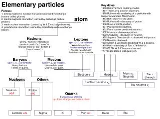
Main topics • Scanning Transmission Electron Microscopy (STEM): - basic principles - a little history • Single atom imaging and spectroscopy • Summary C and O in BN Si3N4 Si in graphene
STEM - an instrument for imaging and analyzing atoms An electron probe with ~1010 electron per second that’s smaller than an atom is formed and scanned across the sample. Many types of fast electron – single atom interactions can be detected, typically in parallel. 3 2 4 Key primary signals and detectors: 1 • Elastic scattering from the • atomic nucleus (Rutherford scattering): high angle ADF • Inelastic scattering from electrons: electron energy loss spectrometer (EELS) 3) e- wavefront reconstruction (holography): 2D camera 4) Inelastic scattering from the nucleus: high resolution EELS
STEM - an instrument for imaging and analyzing atoms An electron probe with ~1010 electron per second that’s smaller than an atom is formed and scanned across the sample. Many types of fast electron – single atom interactions can be detected, typically in parallel. 2 4 Key secondary signals and detectors: CL detector 1 1’) Secondary electrons (SE) arising from various scattering processes: low-energy electron detector 4’ 2’ 3’ 2’) X-rays arising from de-excitation of inner shell hole: X-ray spectrometer (EDXS, WDS) X-ray detector 1’ SE detector 3’) Auger electrons arising from de-excitation of inner shell hole: low-energy electron detector with energy filtering • 4’) Optical, infrared + UV photons arising from various de-excitiation processes: cathodoluminescence (CL) detector There are many signals, and this why the STEM approach is very powerful.
The father of modern STEM: Albert Crewe Albert Crewe showing single U atoms in a Z- contrast image of stained DNA (1970) Chicago 40 kV STEM
Washington state, USA: 1st EM outside of Europe… Washington State EM history continued: 1998: Nion Co. started. It makes correctors for VG STEM microscopes. 2007: Nion starts delivering complete STEMs.
… and now the home of a revolutionary new STEM Nion’s first 200 keV, 0.53 Å resolution STEM is shipped to CNRS Paris-Sud (in Orsay). Members of the Orsay STEM group (Christian Colliex, Odile Spehan, Katia March, Marcel Tence) and Nion’s Niklas Dellby with Orsay’s new 200 kV UltraSTEM
Nion UltraSTEM™ 200 Fully modular and thus very flexible. Operating voltage range 20-200 kV. UHV at the sample (<10-9 torr; <10-7 Pa). Aberration corrector 2 Ultra-stable, friction-free sample stage Efficiently coupled EELS Aberration corrector 1 UltraSTEM200* Described in: Krivanek et al. Ultramicroscopy 108 (2008) 179-195 and Dellby et al. EPJAP 2011. More info at www.nion.com. *instrument shown: CNRS Orsay, France
Other major Nion firsts 2000: first commercial aberration corrector in the world delivered 2001: sub-Å electron probe 2007: atomic-resolution EELS elemental mapping 2009: atomic-resolution images of graphene and monolayer BN 2011: EELS fine structure from single light atoms 2012: X-ray spectrum from a single atom EDXS of one Si atom EELS of one Si atom C-K Si-K C and O in BN
STEM probe size in the aberration-corrected era Graph shows probe size for probe current Ip = 0.25 Ic dprobe(Cc) ~ (Cc δE) 1/2 / E*o3/4 Ic = coherent probe current (~0.1-0.5 nA for CFEG) uncorrected STEM, Cs = 1 mm Resolution reached in the Nion 200 keV column (and illustrated in this talk) dprobe(C7,8) ~ C7,81/8 / E*o1/2 Area of great current interest, by Matt Chisholm, Juan Carlos Idrobo, David Muller, Quentin Ramase, Kazu Suenaga, Wu Zhou, Jannik Meyer, Ute Kaiser, David Bell and others.
STEM probe size in the aberration-corrected era Graph shows probe size for probe current Ip = 0.25 Ic Ic = coherent probe current (~0.1-1 nA for CFEG) dprobe(Cc) ~ (Cc δE) 1/2 / E*o3/4 uncorrected STEM, Cs = 1 mm Resolution reached in the Nion 200 keV column (and illustrated in this talk) dprobe(C7,8) ~ C7,81/8 / E*o1/2 Area of great current interest: work by Kazu Suenaga, Jannik Meyer, Ute Kaiser, David Bell and others. For the full expressions describing the above curves, see Krivanek et al.’s chapter in the just-published Pennycook-Nellist STEM volume (Springer).
HAADF imaging of ß-Si3N4 La grain boundary dopants 0.94 Å Nitrogen columns, separated by only 0.94 Å from Si columns, are clearly visible. Nion UltraSTEM200, 200 kV. Courtesy Tim Pennycok, ORNL.
-1 (0.12 nm) HAADF imaging of gold particles at 40 and 200 keV 40 keV: 1.23 Å lattice planes well resolved (Nion UltraSTEM200, Orsay, France) The image was acquired in the so-called “second zone” OL mode, with 2 beam crossovers in the objective lens. This lowered Cc and gave better than the regular imaging mode. Image recorded by N. Dellby. Dellby et al, EPJAP (2011), DOI: 10.1051/epjap/2011100429
HAADF imaging of gold particles at 40 and 200 keV 40 keV: 1.23 Å lattice planes well resolved (Nion UltraSTEM200, Orsay, France) 200 keV: 0.53 Å information transfer that’s independent of the scan direction (Nion UltraSTEM200) regular scan scan rotated by 90°
Single-wall carbon nanotube imaged at 60 keV MADF image of single wall carbon nanotube, Nion UltraSTEM100. Masking a set of reflections in the FFT allows the front and the back of the nanotube to be visualized separately. Image courtesy Matt Chisholm, ORNL. Microscope is housed in a soft steel box, shown here with one of its side doors open. The box makes the microscope relatively insensitive to external disturbances. It also serves as a bake-out enclosure.
MAADF images of graphene taken 2 minutes apart Medium angle annular dark field (MAADF) STEM images of a graphene edge, recorded 2 minutes apart. Nion UltraSTEM, 60 keV primary energy. Configuration changes at the edge are nicely documented, a single heavier adatom (probably Si) is seen. Recorded in July 2009.
EELS atomic-resolution chemical mapping (2007) EELS chemical maps of La0.7Sr0.3MnO3/SrTiO3 multilayer structure 40 mr illum. half-angle 0.4 nA beam current ~1.2 Å probe >80% efficient EELS coupling 64x64x1340 voxel spectrum-image 7 msec per pixel, i.e. 29 sec total acquisition time 10 sec additional processing time i.e., <1 min total time Nion UltraSTEM100, 100 keV La (M) Ti (L) RGB Mn (L) 5 Å Muller et al., Science 319, 1073–1076 (2008)
Imaging different chemical species separately EELS chemical mapping: imaging of oxygen and other sub-lattices due to specific chemical elements in LaMnO3. Octahedral rotations in the O sub-lattice are clearly seen. Nion Ultra-STEM100, Gatan Enfina EELS, 100 keV. 1 nm 1 nm O-K Mn-L2,3 La-M4,5 RGB composite Courtesy Maria Varela and Steve Pennycook, ORNL.
Result of DFT calculation overlaid on an experimental image C ring is deformed N Cx6 B O Longer bonds Na adatom BN monolayer with impurities imaged by MAADF C O C
Si substituting for C in monolayer graphene 2 Å Si Si Si Si Si N Si Si Si Si in topologically correct graphene Si at and near topological defects Si at graphene’s edge Medium angle annular dark field (MAADF) images. Nion UltraSTEM100, 60 kV. Image courtesy Matt Chisholm, ORNL, sample courtesy Venna Krisnan and Gerd Duscher, U. of Tennessee.
Si substituting for C: 2 structures are possible 2 Å Si Si in defect-free graphene strains (and buckles) the foil. (courtesy Matt Chisholm) Si in defective, but less strained graphene is more stable. (15 images added together, no other processing, courtesy Wu Zhou and Juan-Carlos Idrobo)
Binding of a single Si atom in a stable defect structure Si-L edge EELS from single Si atom Exp. Exp.: adding together the signal of the pixels corresponding to the Si atom in the graphene spectrum-image N C Si Nion UltraSTEM100, 60 keV. Courtesy Juan-Carlos Idrobo and Wu Zhou, ORNL
Simultaneous EELS and EDXS from a single Si atom EELS of single Si atom on graphene ADF image of 2-3 graphene layers recorded after spectra were acquired. Arrow points to a tracked impurity atom. EDXS of single Si atom Si-K C-K EELS and EDXS data recorded simultaneously. Ip = 100 pA, 90 s acquisition. E (keV) Nion UltraSTEM100, 60 keV, Daresbury UK. Gatan Enfina EELS, Bruker SDD EDXS. Q. Ramasse, T.C. Lovejoy, O.L. Krivanek et al., to be published.
Summary • The ability to image and analyze matter atom-by-atom was always inherent to the nature of the electron-matter interaction, and it’s now finally available. • We are able to perform atom-by-atom analysis because we have: ultra-bright electron guns aberration-corrected electron optics ultra-stable electron microscopes ultra-high vacuum at the sample • The ability to analyze matter atom-by-atom has arrived just in time: atom-by- atom is how we now make the smallest devices. • Being small and nimble is an advantage when it comes to creating revolutions. EDXS of one Si atom C-K Si-K EELS of one Si atom Si in graphene