SIDECAR ASIC @ ESO
SIDECAR ASIC @ ESO. Reinhold J. Dorn and the IR detector department. Instrumentation Division - European Southern Observatory. What is a SIDECAR ASIC ?. SIDECAR™ - system image, digitizing, enhancing, controlling, and retrieving - ASIC - Application Specific Integrated Circuit -.

SIDECAR ASIC @ ESO
E N D
Presentation Transcript
SIDECAR ASIC @ ESO Reinhold J. Dorn and the IR detector department Instrumentation Division - European Southern Observatory
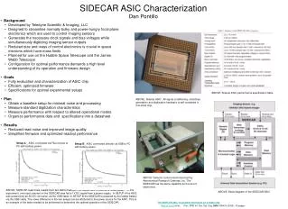
What is a SIDECAR ASIC ? SIDECAR™ - system image, digitizing, enhancing, controlling, and retrieving - ASIC - Application Specific Integrated Circuit - The ASIC is a controller on a single Chip designed for use in Teledyne Imaging Sensors FPAs including the 2048 x 2048 HAWAII-2RG™ and other detectors
ASIC @ ESO – LCC package < 100 mW at 100 kHz 32 – channel operation Chip dimensions ~ 22mm x 15 mm using deep submicron CMOS processing Only requires one power supply, one fixed reference and one master clock for operation
ESO- ASIC cryogenic setup inside cryostat JADE card on the outside
SI-PIN/Visible hybrid Hawaii2RG detector Picture of the Hybrid Visible Silicon Imager (HyViSI) used for testing the SIDECAR ASIC It is a complementary metal oxide semiconductor (CMOS) alternative to charge coupled devices (CCDs) for photons at optical wavelength. 2k x 2k format with 18 micron pixels A silicon pin hybrid detector has close synergy with IR (HgCdTe) detectors. Main difference: SI-PIN array is a fully depleted bulk detector , IR array is a per pixel depleted detector.
ESO- ASIC performance improvements STEP 1 STEP 2 STEP 3 STEP 1: Supply clean 5V to JADE card and insulate USB connection with Fiber converter STEP 2: Measure right conversion factor and remove channel offsets with reference pixels, ground ASIC substrate to analog ground STEP 3: Fix and tune microcode and ASIC for low noise performance Images: ASIC / HyViSI single double correlated reads
HyViSI / ASIC conversion factor • Interpixel coupling attenuates poisson noise and introduces error of up to 50 % for the conversion factor. • IR detector lab makes first prove with FE-55 measurements on HyViSI detector. • ESO also developed direct method to measure nodal capacitance (see G. Finger this conference). Wrong Shot noise: Cnode=28.5 fF Capacitance comparison: Cnode=13.9 fF In this case the shot noise method is wrong ! Histogram of Hawaii-2RG Si-PIN HyViSI array exposed to Fe55 X-ray source. The same data set is plotted with nodal capacitances derived from capacitance comparison method (solid histogram) and shot noise method (dashed histogram).
HyViSI pixel crosstalk – optical spot test Focused optical spot Photometric analysis Normalized signal surface plot • Due to interpixel capacitance 43.5 % of the total energy is seen in neighboring pixels (Vsub=10V) • Coupling to closest neighbor pixel is around 8 to 10 %. • Effect includes deterministic scattering mechanism and diffusion (1.5%).
HyViSI / ASIC conversion factor (FE-55) FE-55 is a radioactive source that emits X rays at three energy levels(5.9 KeV (Mn K line), weaker peak at 6.5 KeV (Mn K) and the third at 4.12KeV (K escape line). When these Xrays are absorbed by silicon they produce large photoelectron events K 1620 electrons, K1778 electrons and the K escape peak 1133 electrons. The K line was used to calibrate the conversion gain (needs photometric analysis) FE-55 events on the detector FE-55 source installed on the window HyViSI FE-55 histogram:Conversion factor 1.47 e/ADU
HyViSI / ASIC conversion factor (Histograms) Conversion factor 1.47 electrons / ADU Conversion factor 0.54 electrons / ADU
HyViSI / ASIC conversion factor (calculation) The ASIC Pre-Amp Amplifier is capable of gain -3dB to 27dB gain in 3dB steps. A gain setting of 9db gives corresponds to a gain of 2.83. How is conversion gain and nodal capacity related? Electronic gain of the preamp is 2.83 and the nodal capacitance is 13.9 fF. and the conversion factor is: with c is the conversion factor in electrons/ADU s is ADC sensitivity 3.3V/216= 50 x10-6 Volt/ADU g is electronic gain of the preamp G is conversion gain in electrons/Volt q is the electron charge 1.60218 x 10⁻¹⁹ C or As This is consistent with a conversion factor 1.47 e/ADU from the HyViSI FE-55 histogram.
HyViSI quantum efficiency In the past the Quantum efficiency measurements have been interpreted wrong due to the overestimation of the nodal capacity (conversion factor). Now measured data fits well to modeled values from Rockwell. In the near IR the QE depends on operating temperature. As the temperature get lower, the photon absorption length increases (bigger Si bandgap). Teledyne modeled data
HyViSI / ASIC Refpixel subtraction Due to KTC noise at the input of the ASIC preamp the 32 channels show a slightly different offset level for a difference image. This can be compensated by subtracting the mean of the reference pixels on the top or bottom for the corresponding channels. DC read without ref. pixel subtraction DC read with ref. pixel subtraction i.e. for the first channel: ch1=DC1[0:63,0:2047]*1.0 ch1ref=ch1[0:63,0:3]*1.0 meanvalue=mean(ch1ref) ch1clean=ch1-(meanvalue)
ASIC preamp functional diagram • This is a simplified schematic representation of the Amplification block. • The open/closed condition of each switch depends on the state of the Pre-Amp with has • 4 operational states. • An internal state machine regulates the Pre-Amp state transitions and the correct position • of the switches.
ASIC preamp V1 to V4=GND Noise Stdev=3.6 ADU The ASIC preamp can be used to measure noise of the operating voltages by means of feeding desired voltages to the preamp inputs. This allows fine tuning of voltages for low noise performance. By setting all inputs to ground the ADC conversion noise can be measured. Present microcode is optimized for low power consumption of the ASIC but higher noise. Fine tuning buffers, voltages and ADC gives lower noise but increases power consumption.
ASIC @ ESO - two ways to operate the ASIC now available • ASIC, JADE2 card, bare MUX • Windows based system • USB2 link to PC • Detector is read via IDE and • IDL interface • ASIC, ESO card, bare MUX • LINUX based system • Fiber link to PC • Detector is read with NGC software • (NGC GUI, RTD, etc.)
Picture of the NGC@ASIC interface card Fiber interface VIRTEX 2 pro Power 5 Volts Connector to ASIC see M. Meyer this conference
NGC@ASIC Communication Channel to/from ASIC and Receiver of Science Data from ASIC all mapped on NGC Fiber link At present the communication link between the ASIC and the NGC interface is a single LVDS line having a bandwidth of 50MBit. This limits the minimum readout time of the Hawaii2RG array to 1.7 seconds. In a next step the VHDL code of the NGC interface will be changed to make use of 16 parallel data lines thus increasing the bandwidth to ~ 400Mbit. This will reduce the readout time of the Hawaii2RG to 200 ms.
NGC and ASIC Backend Back-End PCI is a module with connection to a 64 Bit PCI bus. • Function is based on the XILINX Virtex Pro FPGA • The slave IF is used for communication. • The master IF is used for video data DMA transfers to PCI. • Two RocketIO transceivers ( 2.5 GBit each) are used for Communication and data transfers, other options to increase bandwidth are possible ( one FPGA contains 8 transceivers – space limit for PCI card size might be four ). Fiber Duplex Connection NGC PCI Backend card ASIC interface card
Picture of the IR lab obtained with ESO card, H2RG detector and ASIC ASIC implementation - NGC GUI see J. Stegmeier this conference
ASIC / HxRG code ASIC / HxRG code provides all functionality possible with HxRGs • Multiplexer type (H1RG, H2RG, or H4RG) and more • Optical and IR HxRG detectors • Number of detector outputs used (1,2,4,16,32) • Number of SIDECAR ADCs averaged per output (1,2,4, 8) • Cold or Warm operating temperature • Pre-Amp gain, reset scheme, reference and current sourcing • Buffered or Unbuffered mode on HxRG detector • Horizontal clocking and pixel reset scheme (line by line, pixel by pixel, global) • DC, Up the ramp or Fowler exposure settings (free to program) • Window mode
Performance: Readout noise DC read DCS with HyViSI and ASIC: Readout noise 7 electrons with 0.54 e/ADU conversion factor Performance: Readout noise 30 Fowler pairs 30 Fowler pairs with HyViSI and ASIC: Readout noise 2.7 electrons with 0.54 e/ADU conversion factor
Highlights • ASIC now embedded in ESO hard and software standards • Development of new interface card and software development under LINUX– replacing the JADE USB2 card • Tested SIDECAR ASIC in 32 channel mode with a H2RG (HyViSI) from Teledyne Scientific Imaging reading at a pixel rate of 100 KHz operating at cryogenic temperatures. • ASIC delivers “almost” equal noise performance compared to NGC and IRACE with HxRG arrays • Demonstrated read noise as low as 7 electrons for a DCS and as low as 2.7 electrons with 30 Fowler pairs. • The ASIC readout electronics facilitates a great simplification to system design. • Full systems needs less than 3 Watts and only one 5 Volts power supply • ASIC systems including power supply less then 1 Kg
HyViSI readout noise Readnoise was measured as a function of Folwer pairs at different temperatures. • Strong temperature dependence which can not be explained by Johnson noise but follows 1/sqrt(n) for Fowler sampling. The reason known but has been addressed to the manufacturer. • 6 electrons for a single DC • read (readtime ~1 sec) • as low as 1.8 electrons for • 30 Fowler pairs (readtime ~25 sec) • (at 115 Kelvin with a conversion gain measured with the FE-55 method). • Note that the readnoise does not improve with more samples.
330Ke HyViSI – Residual image Persistence is the remaining signal apparent in a series of dark exposures after the detector has been exposed to a bright radiation source. This residual image is a function of flux of the previous exposure. 25s 75s 150s 225s 475s Decay of residual image intensity as a function of time and prior signal flux.
HyViSI dark current Dark current bottoms out at 3x10⁻³ electrons/sec below 140 Kelvin for this eng. device. Darkcurrent values might be lower with science grade devices but for the eng. grade the dark current is around a factor 10 higher than that of scientific CCDs [green curve].
SI-PIN/Visible hybrid device architecture • Main difference: • SI-PIN array is a fully depleted bulk detector • IR array is a per pixel depleted detector. • Properties of SI-PIN arrays: • 100 % fill factor • High electric field strength • (Vsub ~10 Volts) • Lower integrating node • capacity than IR detectors • => lower noise • Fully depleted bulk => good QE • All features of the Hawaii2RG • multiplexer can be used Note that Hybrids differ substantially from monolithic CMOS where photon detection and readout take place in the same piece of silicon.
HyViSI pixel crosstalk – single pixel reset Single pixel reset Photometric analysis Normalized signal surface plot Note: Central pixel value reduced to 0.3 Array is uniformly illuminated with high flux and by resetting a single pixel with the guide mode feature of the 2RG mux its value is set to zero. • Due to interpixel capacitance 42 % of the total energy is seen in neighboring pixels. • Coupling to closest neighbor pixel is around 8 to 10 %. • Effect is deterministic scattering mechanism and not diffusion

