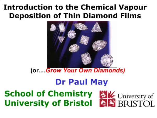
Download
1 / 24
240 likes | 393 Vues
Resonant field emission through diamond thin films Zhibing Li. 1. The problem 2. The picture 3. A simple model 4. Solution 5. Emitted current 6. Discussions. 1. The problem. A model for this system The emitted current?

E N D
Resonant field emission through diamond thin filmsZhibing Li 1. The problem 2. The picture 3. A simple model 4. Solution 5. Emitted current 6. Discussions
1. The problem • A model for this system • The emitted current? • Can one expect any novel (useful) feature in amorphous diamond ultra-thin films? Vacuum
2. The Picture • experiment hints • The film is an insulator of nano scale. ---- Quantum effects would be important. • The amorphous diamond locally likes a crystal but is disordered in long-range. ---- The band structure is similar to the diamond crystal but both valence band and conduction band have band tails of local states (Mott 1967). • Emission is enhanced by dopants of N and Li etc. • Low threshold voltage is detected in polycrystalline diamond.
E0 10 0 • In a ultra-thin film, resonant tunnelling is possible • Randomness tends to create local states (P.W. Anderson 1958) E0 - VA local states (empted) local states (occupied)
What create the local states? • the randomness of amorphous diamond • the grain boundaries of polycrystalline • defects, impurities, and stack faults etc • The scattering mainly is caused by (i) film boundaries; (ii) local potentials corresponding to the local states.
0 d b Typical scales of the potential The energy of injected electrons ~
3. A simple model One dimension model. The effect of local states is represented by a series of delta potentials, each of which has a bound state.
The hamiltonian E0 is the difference between the bottom of conduction band and the energy of the local state
4. The solution It is an exercise of quantum mechanics. 1) Solution for a linear potential The Schoedinger equation is Let , , one has
i) Classical region Let one has This is a 1/3 order Bessel equation, the solution is Two independent wave-function of energy E are
ii) Non-classical region Let The Schoedinger equation becomes It is a 1/3 order modified Bessel equation. The solutions are Two independent wave-functions are
iii) Matrix representation In classical region, a general state of fixed energy E can be written as In the matrix representation, In the non-classical region, iv) Connection condition at the transition point x0
2) Include the random potential j 0 1 2 …… i x0 i+1 i+2 ...... n d y0 b C0 C1 Ci Bi+1 Bi+2 Bn Bn+1 Cn+2 Bn+3 At there is a local potential At x0 electron crosses from non-classical region to classical region, at a it enters the non-classical region again and gets out at y0. Define a matrix: , ,
Connection conditions i) In non-classical region j Cj-1 Cj In matrix representation Define matrix
Then the connection condition is ii) In classical region Replace by in the matrix , one has iii) Transmission coefficient Define
Where , with the wave numbers of incident and transmitted electrons respectively, is the longitudinal mass of electron in Si. The transmission coefficient is given by 3) Average over n For specification, assume n follows the Poisson distribution where is the mean value of n.
For a given n, we generate m positions In the case of uniform distribution, those positions regularly locate in the range (0, d) with separation . The average transmission coefficient is In the case of random distribution, the positions of delta potentials are generated by Monte Carlo method. Average over samples of positions should be done.
5. Emitted current The number of electrons with energy between E~E+dE and with normal energy between Ei~Ei+dEi impinging on the diamond film from the semiconductor (heavy dopped) is is the transversal mass of electron in Si. The number of electrons emitted per unit area per unit time with total energy E~E+dE , that is the so-called total energy distribution (TED) of the emitted electrons, is given by
The emitted current is Integrate with respect to E first, one attains
6. Discussions • Replace the potential by a more realistic one. • For thick film, defect density should be used instead of isolate defects. • 3D • The defects have importance consequences. The simple model shows the possibility of emission enhancement by defects (such as doping of nitrogen) • Resonance transmission is the most idea case for applications