Electroless Copper Deposition on ABS Plastics for Enhanced Conductivity
Explore the process of converting non-conductive plastic surfaces into conductive layers using aluminum or aluminum-carbon pastes for subsequent copper deposition. This study offers insights into enhancing adhesion and conductivity for various applications.

Electroless Copper Deposition on ABS Plastics for Enhanced Conductivity
E N D
Presentation Transcript
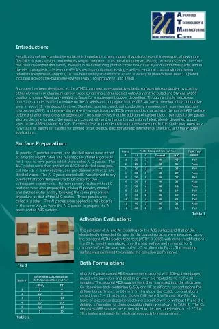
Introduction: Metallization of non-conductive surfaces is important in many industrial applications as it lowers cost, allows more flexibility in parts design, and reduces weight compared to its metal counterpart. Plating on plastics (POP) therefore has been developed and widely involved in manufacturing printed circuit boards (PCB) and automobile parts, and in the electromagnetic interference (EMI) shielding application. Having excellent electrical conductivity and being relatively inexpensive, copper (Cu) has been widely studied for POP and a variety of plastics have been Cu plated including acrylonitrile-butadiene-styrene (ABS), polypropylene, and Teflon. A process has been developed at the ATMC to convert non-conductive plastic surfaces into conductive by coating either aluminum or aluminum-carbon black containing enamel pastes onto Acrylonitrile Butadiene Styrene (ABS) plastics to create Aluminum-seeded surfaces for a subsequent copper deposition. Through a simple electroless procedure, copper is able to reduce on the Al seeds and propagate on the ABS surface to develop into a conductive layer in about 10 min deposition time. Standard tape test, electrical conductivity measurement, scanning electron microscope (SEM), and energy dispersive X-ray spectroscopy (EDS) were used to characterize the coated ABS surface before and after electroless Cu deposition. The study shows that the addition of carbon black particles to the pastes shorten the time to reach the maximum conductivity and enhance the adhesion of electrolessly deposited copper layer to the ABS substrate surface. The electroless copper deposition process developed in this study may open up a new route of plating on plastics for printed circuit boards, electromagnetic interference shielding, and many other applications. Surface Preparation: Al powder, C powder, enamel, and distilled water were mixed at different weight ratios and magnetically stirred vigorously for 1 hour to form pastes which were called Al-C pastes. The Al-C pastes were then applied on ABS boards that were pre-cut into ~5 × 5 cm2 squares, and pre-cleaned with soap and distilled water. The Al-C paste coated ABS was allowed to dry overnight at room temperature to be ready for the subsequent experiments. For comparison, pastes without C particles were also prepared by mixing Al powder, enamel, and distilled water and by following the same preparation procedure as that of the Al-C pastes. These pastes were called Al pastes. The Al pastes were applied on ABS boards in the same way as were the Al-C pastes to prepare the Al paste coated ABS surface. Table 1 Adhesion Evaluation: The adhesion of Al and Al-C coatings to the ABS surface and that of the electrolessly deposited Cu layer to the coated surfaces were evaluated using the standard ASTM Scotch-tape test (ASTM D 3359) with minor modifications – a 25 kg weight was placed onto the test surface and remained for 5 minutes before the tape was pulled off, as shown in Fig. 1. The resulting surface was examined to evaluate the adhesion performance. Bath Formulation: Al or Al-C paste coated ABS squares were scoured with 300-grit sandpaper, rinsed with tap water, and dried in an oven pre-heated to 40 ºC for 30 minutes. The scoured ABS squares were then immersed into the electroless Cu deposition bath containing CuSO4 and HF at different concentrations for different time (from 1 to 60 min). In this study, the CuSO4 concentrations varied from 5 ~ 15 wt%, and those of HF were 5 wt% and 10 wt%. Two types of electroless deposition bath were studied with or without HF and the detailed information of these deposition baths was shown in Table 2. The Cu deposited ABS squares were then dried in the oven pre-heated to 40 ºC for 30 minutes and ready for electrical conductivity measurement. Fig. 1 Table 2
b Electroless Copper Deposition on Aluminum-seeded ABS Plastics Dapeng Li Department of Materials and Textiles University of Massachusetts – Dartmouth Kate Goodwin Department of Chemistry and Biochemistry University of Massachusetts – Dartmouth Chen-Lu Yang Advanced Technology and Manufacturing Center University of Massachusetts – Dartmouth Electrical Performance: Shown in Table 3 are the electrical resistance measurement of both Al and Al-C paste coated ABS after electroless Cu deposition for different time. At 1 min deposition time, both Al and Al-C paste coated ABS samples show immeasurable resistance, indicating their poor conductivity. After 2 min deposition, the Al-C paste coated ABS becomes conductive with a measured resistance of 846.9 ± 714.4 Ohm/cm2, while the Al paste coated sample still yields immeasurable resistance, and it is not conductive until deposited for 5 min (25.1 ± 31.5 Ohm/cm2). Table 3 Copper Deposition: Scanning electron microscope was used to investigate the deposition of copper on Al-C paste coated ABS samples. Fig. 2 shows the SEM images of Al-C paste coated ABS before (a) and after scouring (b), and of the scoured ABS after electroless Cu deposition for different time. (c) 1 min, (d) 2 min, (e) 5 min, (f) 60 min. (a) (b) (c) (d) (e) (f) Fig. 2 Fig. 3 Metal Identification: As illustrated in Fig. 3, the EDS spectrum of the scoured ABS surface is dominated by Al at 1.487 keV (Kα, red arrow in the Fig.). With the increase of deposition time, the Al peak decreases and is replaced by three Cu peaks at 0.930 keV (Lα), 8.041 keV (Kα), and 8.905 keV (Kβ), and at the 60 min deposition time, the entire surface appears to be dominated by Cu. These are evident that Cu2+ has been reduced by the Al particles seeded on ABS and gradually propagated to cover the surface over time until a maximum coverage level is reached to lead to the minimum resistance. Fig. 4 Shows the composition change of the Al-C paste coated ABS surface as a function of deposition time. Three randomly selected areas of each ABS sample were EDS analyzed to obtain the compositions. Fig. 4
a4 a1 a2 a3 c4 c1 c2 c3 a1 a2 a3 d1 d2 d3 d4 b1 b2 b3 University of Massachusetts Dartmouth Chapter of Sigma Xi, the Scientific Research Society 15th Annual UMass Dartmouth Research Exhibition April 28-29, 2009 EDS Microanalysis: Fig. 5 shows the EDS maps of the Al paste coated ABS surface before (a1-a3) and after scouring (b1-b3), and the scoured ABS surface after 1 min (c1-c4) and 60 min (d1-d4) of electroless Cu deposition (Bar length = 60 µm). Green: Al, Red: C and, Blue: Cu (Same for all other EDS maps). Fig. 5 The deposition of Cu on Al-seeded ABS surface has changed the elemental distribution. Fig. 5 c1-c4 show the propagation of Cu on ABS surface over deposition time. One can see clearly from Fig. 5 c1-c4 that Cu particles start growing on the surface of several Al seeds, but only part of the area of those seeds is covered by Cu at that deposition time. After 60 min, however, a continuous Cu layer has developed to almost fully cover the surface, leaving only a few scattered spots remained “naked” (Fig. 5 d4). Fig. 6 Cross section of the Al-C paste coated ABS was also EDS mapped (Fig. 6 a2-a4). A Cu layer of about 10~15 µm thick has been formed on the top surface (Fig. 6 a4) and such a thickness appears to agree with the height of Cu particles, namely, a single layer of Cu particles is deposited on the ABS surface. Conclusions: Al or Al-C containing enamel pastes were coated onto ABS plastic to create Al-seeded surfaces onto which Cu could be readily deposited through a simple electroless procedure, converting the non-conductive plastic surface into conductive. Standard tape test, electrical conductivity measurement, SEM, and EDS were used to characterize the coated ABS surface before and after electroless Cu deposition. It was found that addition of C particles to the pastes shortened the time to reach the maximum conductivity and enhanced the adhesion of electrolessly deposited Cu layer to the substrate. The electroless Cu deposition process developed in this study may open up a new route of deposition on plastics (POP) for printed circuit boards, electromagnetic interference shielding, and many other applications. We realized that the following studies are important to optimize the paste formula and to elucidate the mechanism of Cu growth on the Al seeds: • The role HF plays in enhancing the Cu deposition; • The role C plays in improving the conductivity at short deposition times and enhancing the adhesion of the deposited Cu layer to the substrate.