Download
1 / 28
701 likes | 2.61k Vues
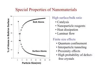
Nanomaterials – Electronic Properties. Keya Dharamvir. Modifications due to :. Quantum confinement Quantum size effect Energy bands and electronic transition Charge quantization. Nanostructures. Microstructure vs. Nanostructure.

E N D
Nanomaterials –Electronic Properties Keya Dharamvir
Modifications due to : • Quantum confinement • Quantum size effect • Energy bands and electronic transition • Charge quantization
Microstructurevs. Nanostructure • Microstructure Nanostructure • / Bulk • Physics Semi-classical Q. mechanical • Electron’snature Particle-like Wave-like • E or k-space Continuous Discrete • Current Continuous Quantized • Decision Deterministic Probabilistic • Fabrication Micro-fabrication Nano-fabrication • Surface:volume Small Very large • Packing Low Very high
Electrons’ Behaviour in Smaller Sizes • Energy quantization • d ~ Fermi wave length of electron in a metal (lF) • or exciton diameter in a semionductor • Charge quantization • Charging energy (Ec) >> Thermal energy (kT) • Ballistic • d<mean free path (l) Free electron case (3D box): Y = exp(ikr) where k =2pn/L; E= ħ2k2/2m N = 2x (4pkF3/3)/(2p/L)3 = VkF3/3p2 electron concentration N = N/V EF= (ħ2/2m) kF2 = (ħ2/2m)(3p2 N) 2/3; kF = (3p2 N)1/3 lF= 2p/kF= 2p (3p2 N)-1/3
Exciton : e-h pair bounded by attractive electrostatic interaction (H atom-like) E E Conduction band Exciton levels Eg Exciton binding energy: Eex n =2 n=1 Eg Eg-Eex k 0 Valence band • Binding energy: Eex =me4/2eħ2n2 • Bohr (exciton) radius: r = n2eħ2/me2; 1/m=1/me +1/mh • Si Ge GaAs CdSe KCl • Eex (meV) 14.7 3.8-4.1 4.2 15 400 • r (nm) 4.3 11.5 12.4
Quantum Confinement Exciton radius r Energy for the lowest excited state relative to Egap E(R) = h2p2/2mR2 – 1.8e2/2eR … dot R Particle in a box problem • R<< r: Strong Confinement • - 1st term (localization) dominant • - Electron and hole are quantized • - Energy gap ~1/R2 • eg) Si<4.3 nm, Ge<11.5 nm, GaAs<12.4 • R>> r: Weak confinement • - 2nd term (coulomb attraction) dominant • - Exciton confinement character L.E. Brus, J. Chem. Phys. 80, 4403(1984)
1D 2D 3D Density of State: # of states per unit energy range DOS DOS DOS N = 2n/L N =8pn3/3L3 N =2pn2/L2 dN /dE ~ E-1/2 dN /dE = const dN /dE ~ E 1/2 k=2pn/L E = ħk2/2m k =(2mE)-1/2/ħ N = 2xn/L= k/p = (1/pħ)(2mE) 1/2 dN /dE = ((2m)1/2/2pħ)(E)-1/2 • E = ħk2/2m • = ħ/2m(kx2+ky2+kz2) • k is discreet in confinement directions only
Size Effect: Energy Levels and DOS Semiconductor Bulk Nano atom particle 3d 2d 1d 0d CB VB LUMO HOMO DOS Band gap EF Energy Size controlled band gap tuning Discrete Energy levels A.P. Alivisatos, Science271, 933 (1996)
Size Effect:1D-Quantum well states F.J. Himpsel et al, Adv. Phys. 47, 511 (1998)
Size Effect: Optical Spectra • Shift to higher energy in smaller size • Discrete structure of spectra • Increased absorption intensity A.P.Alivisatos, J. Phys. Chem. 100, 13227 (1996)
Size effect:TunableBand Gap Bulk Si = 1.14 eV GaAs =1.5 eV Optical excitation is significantly enhanced, both, in frequency and intensity, in smaller sizes. S. Ogut et al, Phys. Rev. Lett. 79, 1770 (1997)
Energy Band Structure:Energy vs. k Y = Cnfn V = Cn V n (h2/2m)2Y + V Y = E Y Ej=a +2b cos 2pj/N index j = 0, 1, 2 … Define a new index k = 2pj/Na: wave vector E(k) =a +2b coska, Yk = eiknafn: Bloch wave function (symmetry adapted LCAO) a 2 1 0 E …. …. a -2b …. • = 2p/k = 2a • = ∞ a a +2b …. p/a k=0 p/a
Electronic Transition Electric Transition dipole moment mif = <ff |er|fi> • Direct transition (Dk=0) • In phase • Added transition dipole • Electronically • allowed transition ff E mif fi ff • Indirect transition (Dk ≠ 0) • Out of phase • Cancelled transition dipole • Electronically forbidden • but vibronically allowed mif fi p/a k=0 p/a • Band width: overap of wave functions • Slope dE/hdk = hk/m = vg: group velocity of electron
Absorption spectra:Direct and Indirect Transition Electronic absorption spectra for three sizes of CdSe nanocrystals, in the wurtzite (direct) and rock salt (indirect) structures. In each instance the direct gap spectrum is structured and intense, while the indirect gap one is featureless and relatively weaker. The relative absorption efficiencies do not change, despite the concentration of oscillator strength due to quantum confinement.
Size Effect: Enhanced Absorption • For quantum dot, • Energy levels: discrete • DOS: delta function N(E) E k E • DxDp ~ h • x: well defined • p=hk: Not well-defined • k is not an exact quantum • number for QD • Envelope functions sample larger k-space • Overlap of wave functions • - Increased absorption intensity M.S. Hybersten, Phys. Rev. Lett. 72, 1514 (1994)
Photon absorption: Direct vs. Indirect Transition E phonon q hv Eg k Selection rulek’ = k (Dk = 0) k’ = k + q (Dk ≠ 0) Energy relationshiphv = Eg hv = Eg + hv(q) Interaction electronic: two body vibronic: three body Transition rate fast ~ 10 -7 sec slow ~ 10-2 sec Radiative efficiency high low Example GaAs (Eg (dir.) =1.4 eV) Si (Eg (ind.) = 1.1 eV) (Eg (dir.) = 3.37 eV)
P. 26, 27 of doc2 (Optical properties of semiconductor nanoparticles)
P. 18 of doc2 • (optical properties of metal nanoparticles)
Charge Quantization 3 2 1 e e N=0 d • Charging energy: Ec = e2/2C >> kT • At T =300K • kT = 26 meV • C<< 3.1x10⁻¹⁹ F • C = 4pe d • 4pe = 1.1x10⁻¹⁰ J -1 C2m-1 • For charge quantization, • the diameter of dot (d) must be << 28 nm
Tunneling Spectroscopy of InAs QD STM T=4.2K Optical d = 32A S-like P-like U. Banin et al, Nature, 400, 926 (2000) Ec=0.11 eV: single electron charging energy Eg=1.02 eV: nanocrystal band gap
P. 21, 22, 23 of doc2 for Conduction through metal nanoparticles. • P. 30 for Comparison table
Property: Melting Temperature of Nanocrystal A.P.Alivisatos, J. Phys. Chem. 100, 13227 (1996)
Property:Thermodynamic Behaviors of Metal Clusters • As the cluster size decreases, the melting • temperature (Tm) monotonically decreases, • However, when the cluster size is small enough, Tm does not vary monotonically with cluster size. • The absence of a premelting peak in heat capacity curves for some clusers. • Premelting: surface melting, partial melting, orientational melting, and isomerization Y.J. Lee et al, J. Comp. Chem 21, 380 (2000), Phys. Rev. Lett. 86, 999 (2001)