1 mm = 10 6 nm
70 likes | 240 Vues
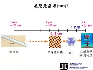
甚麼是奈米( nm)?. 1 mm = 10 6 nm. 1 m = 10 3 nm. 1 Å = 0.1 nm. 1 nm. 0.18 m. 以鐵原子 排列的漢字. 標準尺. 半導體結構. 分子. 1 m. Top-down approach. MEMS. 1 μm. Nanometrology. 0.1 μm. Nanotechnology. Bottom-up approach. 1 nm. Nanometrology. Definition:

1 mm = 10 6 nm
E N D
Presentation Transcript
甚麼是奈米(nm)? 1 mm = 106 nm 1 m = 103 nm 1 Å = 0.1 nm 1 nm 0.18 m 以鐵原子 排列的漢字 標準尺 半導體結構 分子
1 m Top-down approach MEMS 1 μm Nanometrology 0.1 μm Nanotechnology Bottom-up approach 1 nm Nanometrology Definition: Nanometrology is the science of measurement of the dimensions of objects or object features, separations or displacements in the range from 1 nm to 1000 nm ( recommended by: CCL-WGDM7, 1998) Richard P. Feynmen: There’s plenty of Room at the Bottom Christmas, 1959, annual meeting of the American Physical Society at Cal Tech
奈米科技架構 • Biomimetic Sensing • Nano-Bioimplants • Nano-Biolabeling • Nanodevices from Bio 奈米材料 • Super Energy Storage • Nanodisplay Materials & Systems • Nano Information Storage • Nanocatalysts 生技奈米 • Nanoelectronic Devices • Nanophotonics • NEMS 奈米電子 Nanomaterials Nanobiotechnologies Nanoelectronics 加工和製程 量測 模擬 Measurement Support Modeling & Simulation Support Processing And Manufacturing Support • Standards • 3D Measurement • Nanoscale Analysis • Algorithms For Data Mining • Nanotechnology Processing Equipment • Self-Organized Nano Structures • Nano Manipulation • Nano Surface Treatment • Mesoscopic Simulation • Atomistic Simuation • Process Simulation & Design
SPM奈米量測的追溯鏈 Definition of Meter Laser wavelength/ Laser Interferometer I2 Stabilized Laser Metrology Institutes SPM with displacement sensor SPM with Traceable Sensor Uncertainty SRM Standards Calibration with SRM (e.g. SPIP program) General SPM SPM Application in Industry SPM Users Specimen
PC (DI) NanoScope Z DI Ⅲm Controller Z NI A/D PCI-6034E Z Differential Plane Mirror Interferometer DI AFM X L Shape Mirror PI x-y-z Stage P-731K031 X SIOS SP-500 DD Y Y PI E-710K009 Controller RS 232 GPIB IPC (LabVIEW) Stage Control & Data Acquisition SIOS SP-500 DD RS 232 計量型AFM系統示意圖
1 2 9 3 6 4 7 5 8 計量型AFM組合後之照片 1. DI Dimension AFM2. X- Laser Interferometer3. Thermometer4. L Shape Mirror5. Y- Laser Interferometer6. PI Flexure Stage7. Granite & Isolator8. Super-Invar Frame9. Reference Mirror