Download
1 / 16
160 likes | 310 Vues
UV Laser-Induced Damage to Grazing Incidence Metal Mirrors. M. S. Tillack, J. E. Pulsifer, K. Sequoia Mechanical and Aerospace Engineering Department and Center for Energy Research. 3rd International Conference on Inertial Fusion Science and Applications Monterey, CA 9 September 2003.

E N D
UV Laser-Induced Damage to Grazing Incidence Metal Mirrors M. S. Tillack, J. E. Pulsifer, K. Sequoia Mechanical and Aerospace Engineering Department and Center for Energy Research 3rd International Conference on Inertial Fusion Science and Applications Monterey, CA 9 September 2003
Design concept for a power plant GIMM* The reference mirror concept consists of stiff, light-weight, radiation-resistant substrates with a thin metallic coating optimized for high reflectivity (Al for UV, S-pol, shallow q) • * Sombrero and Prometheus studies, ca. 1992.
Key issues were identified for a GIMM* • Shallow angle stability• Damage resistance/lifetimeGoal = 5 J/cm2, 108 shots• Fabrication & optical quality• Contamination resistance• Radiation resistance • S-N curve for Al alloy • * R. L. Bieri and M. W. Guinan, Fusion Technology 19 (1991) 673-678.
We tested several Al fabrication options • Thin films on superpolished substrates – CVD SiC, 2-3Å roughness, 2-3 nm flatness over 3 cm – magnetron sputtering up to 250 nm – e-beam evaporation up to 2 mm• Solid polycrystalline metal – polished – diamond-turned• Electroplated and turned Al
Testing was performed with 25-ns, 248-nm pulses in a controlled environment 420 mJ, 25 ns, 248 nm
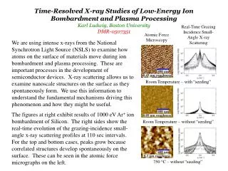
In-situ monitoring helped identify the onset of damage camera • Brightfield beam profiling• Darkfield beam profiling• Surface imaging microscopy in-situ imaging darkfield
Polycrystalline Al is easy to fabricate into a mirror, but has large grains • 1-mm 99.999% pure Al, bonded with CA to 3-mm thick Al alloy • Polished with 5, 1, and 0.04 mm alumina (Al2O3) suspension, or • Diamond-turned on precision lathe (at GA target fab facility) ~25 nm avg. roughness
Polished Al damages due to plastic deformation mechanisms • Exposed for 100 shots in vacuum at 2–5 J/cm2 • Grain boundaries separate • Slip lines extrude within grains 500 X 500 X
Diamond-turned Al exhibits superior damage resistance • Exposed for 50,000 shots in He at 3–4 J/cm2 • No obvious damage • Minimal (if any) grain boundary separation • Polishing appears to introduce impurities and pre-stress the grain boundaries
Thin film deposition is limited by coating thickness and surface defects • Thermal stress, constraints on thickness • Added complexity of substrate and film requirements • Plane stress analysis • 10 mJ/cm2 absorbed • Peak stress at interface ~40 MPa • Yield stress is 10-20 MPa 1 mm coating of Al on SiC
Good coatings were obtained using superpolished CVD SiC substrates • Superpolished CVD SiC: 2-3 Å smooth, 2-3 nm flat• Thin film deposition of Al by magnetron sputtering and/or e-beam evaporation• Up to 2 mm Al has been successfully deposited by e-beam
Thin films are delicate, damage easily and catastrophically 250 nm e-beam23,000 shots @4 J/cm2 1.5 mm e-beam86,000 shots @4 J/cm2
Electroplated Al solves problems with coating thickness and large grains • 50-100 mm Al on Al-6061 substrate• 100,000 shots at 3-4 J/cm2• No discernable change to the surface
Summary • Survival above 100,000 shots has yet to be demonstrated in thin film coatings – damage occurs due to imperfections and high interfacial stresses.• Thicker coatings appear to be more robust, but detrimental effects of grain structures must be avoided.• Thick (>50 mm) electroplated Al on SiC provided the best damage response, due to thickness of coating and small grains. Scale-up and further testing are planned.
Acknowledgements Thanks to the following for their advice and technical support:Jim Kaae et. al, General Atomics microfabrication facilityEd Hsieh et. al, Schafer Corp.Lee Burns, Rohm & Haas Co. Advanced MaterialsWitold Kowbel, MER Corp.Larry Stelmack, PVD Products, Inc.John Sethian and the members of the High Average Power Laser ProgramThis work was funded byUS DOE/DP NNSA
Optic scale-up: multiplexed beams enable smaller, more tolerant final optics FirstPulse LONG PULSE AMPLIFIER (~ 100's nsec) Last Pulse Demultiplexer Array (mirrors) Multiplexer Array (beam splitters) Target FRONT END ( 20 nsec) Only three pulses shown for clarity