Download
1 / 54
540 likes | 644 Vues
Explore the internal structure and components of multi-turn and part-turn actuators with control functions, fieldbus interface, and non-intrusive logging of operating data. Includes diagrams and details.

E N D
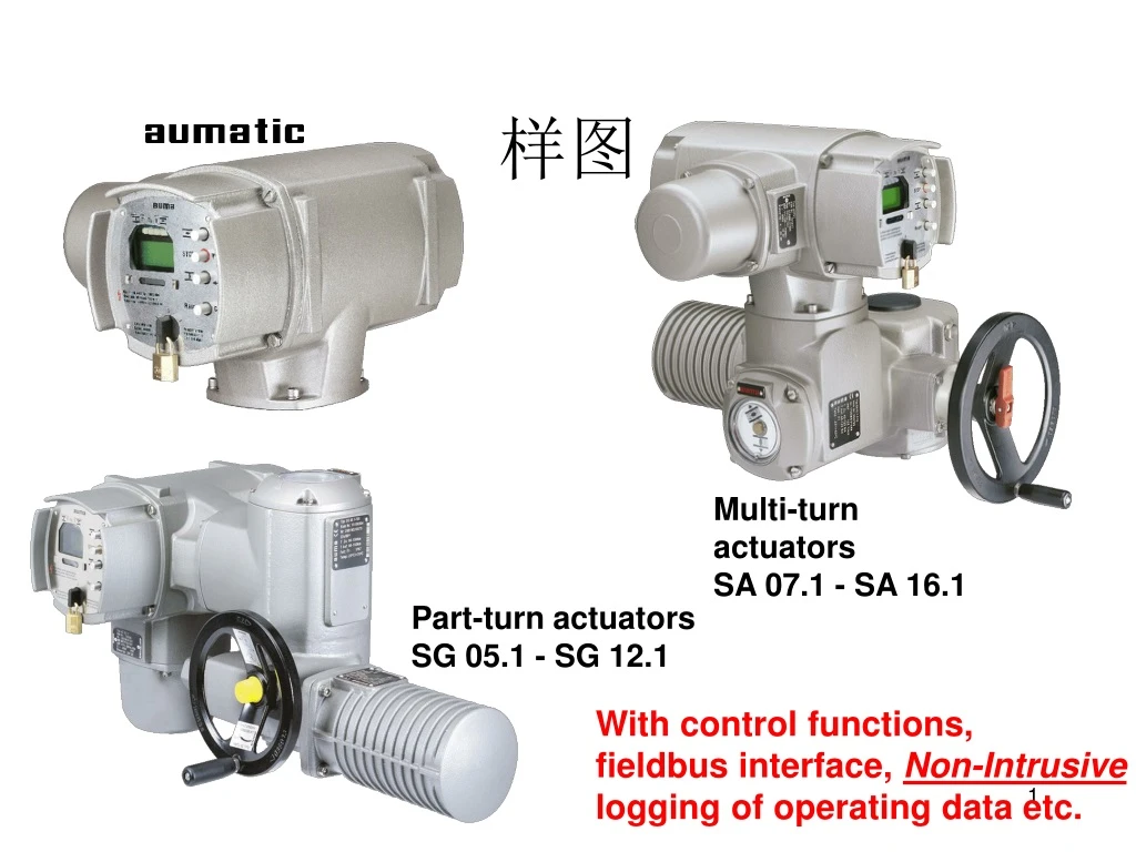
Multi-turn actuators SA 07.1 - SA 16.1 Part-turn actuators SG 05.1 - SG 12.1 样图 With control functions, fieldbus interface, Non-Intrusive logging of operating data etc.
内部结构 • XA 去NORM
内部结构 • XA 去NORM 接触器或可控硅
内部结构 • XA 去NORM • 接触器或可控硅 • 电源板
内部结构 • XA 去NORM • 接触器或可控硅 • 电源板 • 显示屏和编程设备
内部结构 • XA 去NORM • 接口板 • 接触器或可控硅 • 电源板 • 显示屏和编程设备
内部结构 • XA 去NORM • 接口板 • 接触器或可控硅 • 逻辑板 • 电源板 • 显示屏和编程设备
内部结构 • XA 去NORM • 接口板 • 接触器或可控硅 • 逻辑板 • 电源板 • XK去DCS • 显示屏和编程设备
XK去DCS • 就地操作面板带显示屏 • XA去NORM 接口
1. 硬件 For internal use only! • 换向装置 • 接触器或可控硅 • 2.电源板 • 3.继电器板 • 4.逻辑板 • 5.I/O接口板 • 6.显示屏 • 7.总线连接板 • 8.MWG用于 SA or SG执行器
1.1. 可控硅 • 换掉坏硅 • 1,5 kW • 新款 (自2006年5月20周起) • Z039.700/01 THYRISTORMODUL-400VAC • Z041.045 LEISTUNGSTEIL-ETB-AM/AC-THYR-400-1,5kW-m.STECKER • Z041.046 LEISTUNGSTEIL-ETB-AM/AC-THYR-500-1,5kW-m.STECKER • 旧款 K004.679 THYRISTORMODUL-500V-25A-ZS-24VDC • Z007.835 LEISTUNGSTEIL-AM-THYR-400V-1,5 KWZ017.828 LEISTUNGSTEIL-AM-THYR-415V-1,5kWZ027.576 LEISTUNGSTEIL-AM-THYR-500V-1,5kW • 在AC里将接触器换成可控硅 • 1,5 kW • Z032.240 MODUL-AC-THYRISTOR-3x400V/1,5kW • or • Z038.267 UMRUESTSATZ-ETB-AM-THYR-400V-1,5kW • (fits for AM too) V001.634 Back to first slide
1.1. 接触器 • 1,5 kW • K001.015A SCHUETZ-024/024V-50/60Hz-09A-2,2..4KW • 7,5 kW • Z023.877A SCHUETZ-KPL-024/028V-50/60Hz-16A-4..7,5kW K004.278 RC-GLIED-RC-3/022-400V..480V K004.289 RC-GLIED-RC-3/022-500V..690V
BG04 BG02 BG02 BG06 BG02 BG04 电源板 新板从2005年9月起 Z039.666/xx /01 – PRINT-G/U-AC01.1-NT/PF-P380/400/415/500V-S24V /02 – PRINT-G/U-AC01.1-NT/PF-P440/460/480/575V-S24V /03 – PRINT-G/U-AC01.1-NT/PF-P525/600/660/690V-S24V /04 – PRINT-G-AC01.1-NT-P100/110/115/120V-S24V /05 – PRINT-G-AC01.1-NT-P208/220/230/240V-S24V /06 – PRINT-G/U-AC01.1-NT/PF-P208/220/230/240V-S24V /07 – PRINT-G/U-AC01.1-NT/PF-P440/460/480/575V-S115V /08 – PRINT-G/U-AC01.1-NT/PF-P380/400/415/500V-S115V /09 – PRINT-G-AC01.1-NT-P100/110/115/120V-S115V/10 – PRINT-G-AC01.1-NT-P208/220/230/240V-S115V /11 – PRINT-G/U-AC01.1-NT/PF-P208/220/230/240V-S115V 旧板于2005年底废止 Z031.651/xx /01 – PRINT-G/U-AC01.1-NT/PF-P380/400/415/500V-S24V /02 – PRINT-G/U-AC01.1-NT/PF-P400/460/500/575V-S24V /03 – PRINT-G/U-AC01.1-NT/PF-P120/208/230/240V-S24V /04 – PRINT-G-AC01.1-NT-P120/208/230/240V-S24V /05 – PRINT-G/U-AC01.1-NT/PF-P400/660/690V-S24V /06 – PRINT-G/U-AC01.1-NT/PF-P400/460/500/575V-S115V /07 – PRINT-G/U-AC01.1-NT/PF-P120/208/230/240V-S115V /08 – PRINT-G-AC01.1-NT-P120/208/230/240V-S115V /09 – PRINT-G/U-AC01.1-NT/PF-P415/440/480/525V-S24V /10 – PRINT-G/U-AC01.1-NT/PF-P415/440/480/525V-S115V /11 – PRINT-G-AC01.1-NT-P100/110/115/120V-S24V /12 – PRINT-G-AC01.1-NT-P208/220/230/240V-S24V /13 – PRINT-G/U-AC01.1-NT/PF-P208/220/230/240V-S24V /14 – PRINT-G-AC01.1-NT-P100/110/115/120V-S115V /15 – PRINT-G-AC01.1-NT-P208/220/230/240V-S115V /16 – PRINT-G/U-AC01.1-NT/PF-P208/220/230/240V-S115V
3.2. 电源板 BG04 BG02 BG02 BG06 BG02 BG04 新板 (Z039.666/xx) 大图 旧板 (Z031.651/xx) 小图 X9: F3 (24VDC fuse 1.6 AT)(old board has plugs for the fuse F3 (1,6 AT) here) Protect Phase Sequence Detection, X6, X7 X9.1=AC24V not measureable X9.2=AC24V not measureable You can control the voltage on X6, X7 or check the fuse When fuse is blown, the display and the LEDs are dark. X4: F4 (24VAC/115VAC fuse 1,25AT/ 24VAC, 0,315 AT/115VAC) (old board has plugs for the fuse F4 here) X4.1 trafo to F4 X4.2 F4 to X2.5 - X2.3 - X2.1此保险烧断时,屏幕显示过热保护故障 X3: 去逻辑板 (鉴相功能) X3.1=+15VDC to X 7.1 X3.2 Phase 1= 0V (CW) - 15V (CCW) to X 7.2 X3.3 Phase 2=15V (CW) - 0V (CCW) to X 7.3 X3.4= 0V to X7.4 As X7.2 and X7.3 有相同电压时就需要更换板子 X2: 去继电器板 X10 Protected by fuse F4 X2.1=24/115 VAC contactor, TMS(EX) to X10.1 X2.2=24/115 VAC contactor, TMS(EX) to X10.2 Monitoring of motor protection SA/SAEX/SAFM X2.3=24/115 VAC to heater XA 47 X2.4=24/115 VAC to heater XA 47 X2.5= voltage ext. from customer AC 24/115 X2.6= voltage ext. from customer AC 24/115 Jumper between X4.2(F4) - X2.5 - X2.3 - X2.1 X2.6 - X2.4 - X2.2 X7: 备用 (24VDC) Protected by fuse F3 X7.1=+24V has a Jumper to X6.1 X7.2= 0V has a Jumper to X6.2 X8: 去接口板 X6 (24VDC galv. separated) X8.1=+24V DC to X6.1 X8.2= 0V DC to X6.2 Jumper between Rectifier-X5.1-X5.2-X8.1 Rectifier-X5.3-X5.4-X8.2 X6: 去继电器板 (24VDC) Protected by fuse F3 Has a Jumper to X7.1 and X7.2 X6.1=+24VDC to X1.1 X6.2= 0V to X1.2 X5: to XC (24VDC galv. separated) Protected by a self resetting fuse X5.1=+24VDC(most cases analog input) X5.2=+24VDC for customer X5.3= 0V for X5.1 X5.4= 0V for X5.2 Jumper between Rectifier-X5.1-X5.2-X8.1 Rectifier-X5.3-X5.4-X8.2 X1: 初级侧 X1.1=L3 X1.2=L2 X1.3=L1 X1.4=L1 X1.5=L1 X1.6=L1 All arrows start by PIN No. 1
1.3. 继电器板 Z031.695/xx /01 – PRINT-G/P-AC01.1-024AC/SHTZAN/THYR /02 – PRINT-G/P-AC01.1-115AC/SHTZAN/THYR /03 – PRINT-G/P-AC01.1-Ex-024AC/SHTZAN-TMS01.2 /04 – PRINT-G/P-AC01.1-024AC/SHTZAN/THYR-TMS01.2 /05 – PRINT-G/P-AC01.1-115AC/SHTZAN/THYR-TMS01.2 /06 – PRINT-G/P-AC01.1-024AC/SHTZAN/THYR-o.EXT /07 – PRINT-G/P-AC01.1-Ex-024DC/SHTZAN+THRM.OVERCURRENT-RELAIS BG02 BG08 BG02 BG06 BG03 BG02 BG02
3.3. 继电器板 (Z031.695/xx) X4: 来自逻辑板 X5 X9: 电机保护 X9.1=to XA 19 X9.2=to XA 20 (resistance between X9.1 and X9.2 >100 ohm at 23°C) or thermal switch (~ 0 ohm) X4.1=+24VDC signal for relay K2 open X4.2=+24VDC signal for relay K1 close X4.3=Not in use X4.4=Not in use X4.5=+24VDC signal for TMS(EX) reset X4.6= 0V X4.7=+24VDC signal thermal test pass X4.8=Not in use Jumper between X4.1 to X11.2 X4.2 to X11.3 X11: 去可控硅 X11.1= 0V X11.2=+24VDC signal for relay K2 open X11.3=+24VDC signal for relay K1 close X11.4= 0V Jumper between X11.2 to X4.1 X11.3 to X4.2 X10: 来自电源板 X2 (24VAC or 115VAC) Plug X2 has more connection than these X10.1 (24VAC or 115VAC) to X2.1 X10.2 (24VAC or 115VAC) to X2.2 X7: 去接触器 (24VAC or 115VAC) X7.1 NO contact of board relay K1 to the coil of contactor K1 close X7.2 AC common to coil K1/ K2 X7.3 NO contact of board relay K2 to the coil of contactor K2 open Motor Protection BG08 X6: 去逻辑板 X8 (AUMA-Bus) X6.1=CAN L X6.2=CAN H X6.3= 0V X6.4=+24VDC X6.5=+15VDC X6.6=+ 5VDC Jumper 1:1 betweenX6 to X5 BG02 BG02 K3 BG03 Jumper in EX-positon EX-position: Contactors are switched off directly by the thermal switch. In case of an emergency the contactors will be switched off though the parameters say to ignore the thermal fault.normal position: Contactors are switched off by the logic boards software according to the parameters. K1 BG06 K2 X5:备用 (AUMA-Bus) X5.1=CAN L X5.2=CAN H X5.3= 0V X5.4=+24VDC X5.5=+15VDC X5.6=+ 5VDC Jumper 1:1 betweenX5 to X6 BG02 FILTER BG02 X8: 去逻辑板 电机保护) X8.1=+15VDC signal (without fault) X8.2= 0V Output signal X8.1 fromK3 is optically isolated X1: 来自电源板 X6 (24VDC) X1.1=+24VDC X1.2= 0V X3:备用 (24VDC USV) X3.1=+24VDC X3.2= 0V X2: from XC (24VDC) X2.1=+24VDC from customer X2.2= 0V from Customer All arrows start by PIN No. 1 Back to first slide
3.3. 继电器板 (Z031.695/03) 热保护跳闸后能否自动复位 BG02 Motor Protection BG08 BG02 K3 BG03 K1 BG06 K2 短路电机热电阻 FILTER BG02 BG02
1.4. 逻辑板 Z039.670A Kit with logic board, parametrised EEprom and software Eprom works number required! Z031.773/01 (不再使用) to be used only with Eprom Software Z031.922/03-xx current software version: Z031.922/03-11 BG02 BG08 IDC/FL Z031.773/02, Z031.773/03 (for MWG use only) to be used only with Eprom Software Z031.922/05-xx, Z031.922/07-xx (for DeviceNet), Z031.922/08-xx (for Profibus, Modbus, Devicenet, Foundation Fieldbus, supported languages english, german, italien, french, spanish, portugese) current software version: Z031.922/08-01 version Z031.922/08-01 BG04 BG10 BG26 BG06 Plug Z038.305 to deactivate any message of the phase detection. ATTENTION actuator may turn in the wrong direction, because wrong phase sequence will no longer be corrected! After a software update the aumatic can indicate the “INTERNAL WARNING” in S2 and “NO FACTORY SETTINGS” in D3, because of more parameters are used. Please go to menu D4201 (service password is needed) and “SAVE NEW FACTORY SETTINGS” to fix this. Back to first slide
3.4. 逻辑板 1 2 X2: 去NORM (MWG)/ (standard unit)2 different cable assemblies TORQUE X2.1=CAN L to XA 2 X2.2=CAN H to XA 3 X2.3= 0V to XA 6 X2.4=+24VDC to XA 7 X2.5=+15VDCto XA 10 X2.6=+ 5VDC to XA 11 X2.7=RWG signal X2.8=WOEL to XA13 X2.9=WSR to XA10 X2.10=0V X2.11=+24VDC to XA9 X2.12=AS torque signal X2.13=DOEL to XA 6 X2.14=DSR to XA 2 X2.15=0V X2.16=+24VDC to XA1 X2.17=+24VDC X2.18= 0V to XA24 X2.19=(+)RWG to XA23 X2.20=(-) RWG to XA22 X2.21=+5VDC to XA23 X2.22=0V to XA 22 X2.23=POTI to XA21 X2.24=+24VDC X2.25= 0V X6: 备用 (2 dig.inputs/outputs) X6.1=+24VDC X6.2=Input 1 X6.3=+24VDC X6.4=Input 2 X6.5=+24VDC X6.6=Output 1 X6.7=+24VDC X6.8=Output 2 Jumper: X6.1-X6.3-X6.5-X6.7 MWG emergency shut off XC47 and XC48 RWG POT BRAKE AS X3: 电机热保护去继电器板 X8 X3.1=+15VDC (on board) to X8.1 X3.2= 0V to X8.2Thermal fault will be indicated, if X3.1 and X3.2 are disconnected. Connected the tension between X3.1 and X3.2 is 0VDC (15VDC with thermal fault) 数据存储器 (settings, operational data, configuration factory. XT: 实验用 BG02 X5: 去继电器板 X5.1=+24VDC signal for relay K2 open X5.2=+24VDC signal for relay K1 close X5.3=Not in use X5.4=Not in use X5.5=+24VDC signal for TMS(EX) reset X5.6= 0V X4: 就地操作面板 to X3 X4.1 – X4.18 Possible measurement on: X4.17=+5VDC X4.18= 0V BG08 X1: AUMA-Bus to 接口板 X1 Row 2 Not in use V9 LED RED illuminated CPU runningflashing watchdog alarm: Lost connection to master IDC/FL X1: AUMA-Bus to接口板 X1 Row 1: X1.1=CAN L X1.2=CAN H X1.3= 0V X1.4=+24VDC X1.5=+15VDC X1.6=+ 5VDC Program memory (Software) V10 LED SYSTEM OK must flash (green) Setting not visible: On display: D0 PULL UP INPUTS/ SA + SG with MWG(Logic version Z031.922/02-.. and higher). Wrong setting=configuration fault BG04 2 1 X7: 来自电源板 X3 X7.1=+15VDC to X 3.1(voltage from logic X7) X7.2= 0V (CW)|14,2V(CCW)|14,2V(Ph) to X 3.2 X7.3=14,2V(CW)| 0V (CCW)|14,2V(Ph) to X 3.3 X7.4= 0V to X3.4 (GND is from logic X7) As X7.2 and X7.3 has equal voltage the power supply has to be changed. (Ph) Phase error BG10 BG26 BG06 Setting visible: On display: D0 PULL down INPUTS/ SA + SG with standard control unit 25 top 1 26 bottom 2 X8: AUMA-Bus to 继电器板 X6 X1.1=CAN L X1.2=CAN H X1.3= 0V X1.4=+24VDC X1.5=+15VDC X1.6=+ 5VDC LIMIT All arrows start by PIN No. 1 Back to first slide
1.5. 接口板 Standard- Interface 0/4-20mA DeviceNet Back to first slide
2.5. 接口板和连接板 Standard- Interface 0/4-20mA DeviceNet FibreOptic-coupler Back to first slide
3.5. 连接板 Standard- Interface 0/4-20mA DeviceNet Back to first slide
1.5. I/O接口板 BG18 BG12 BG06 top 12 18 4 2 1 bottom 3 1 Z031.408/xx /01 – PRINT-E/A-AC-024DC/115AC-6dE/6dA/2aE/2aA /02 – PRINT-E/A-AC-024DC/115AC-6dE/6dA/1aA /03 – PRINT-E/A-AC-024DC/115AC-6dE/6dA/2aE/2aA-24DC EXT /04 – PRINT-E/A-AC-024DC/115AC-6dE/6dA/1aA-24DC EXT /05 – PRINT-E/A-AC-024DC-4dE/6dA/2aA BG06 /BG04 6 5 4 3 2 1 BG04 BG02 X5: analogue outputs (0-20mA) X3: digital inputs (24VDC/115VAC) X4: digital outputs (relay contacts/ 250V/1A Back to first slide
2.5. I/O接口板 Back to first slide
3.5. I/O接口板 ON 1 2 X4: 数字输出 (relay contacts/ 250V/1A X4.1 K1 to XC 14=NC (fault) X4.2 K1 to XC 15=NO (OK) X4.3 K1 to XC 16=COM X4.4 K2 to XC 17=NC X4.5 K2 to XC 18=NO (DOUT1) X4.6 K2 to XC 19=COM X4.7 K3 to XC 20=NC X4.8 K3 to XC 21=NO (DOUT2) X4.9 K3 to XC 22=COM X4.10 K4 to XC 32=NC X4.11 K4 to XC 33=NO (DOUT3) X4.12 K4 to XC 34=COM X4.13 K5 to XC 35=NC X4.14 K5 to XC 36=NO (DOUT4) X4.15 K5 to XC 37=COM X4.16 K6 to XC 38=NC X4.17 K6 to XC 39=NO (DOUT5) X4.18 K6 to XC 40=COM S1 板子地址 S2 备用setting S1.off / S2.offTwo I/O board can not be used together. X1: AUMA-Bus to接口板 X1 Row 2 Not in use X1: AUMA-Bus to接口板 X1 Row 1: X1.1=CAN L X1.2=CAN H X1.3= 0V X1.4=+24VDC X1.5=+15VDC X1.6=+ 5VDC LED V9 (green) on System OKflashing board defectoff check boards power supply LED’s1. Mode 2. Close 3. Open 4. Stop 5. Emergency 6. Reserve 1 2 BG06 /BG04 X7: 模拟量输入 (0-20mA) X7.1=+24VDC X7.2=analogue input 1 (+) to XK12 X7.3=analogue input 1 (-) to XK13 X7.4 =analogue input 2 (+) to XC 27 X7.5=analogue input 2 (-) to XC 28 X7.6 =+24VDC Jumper Standard: without Jumper Optional: with Jumper The jumpers connect all commons on X4. Without Jumpers relays can be used isolated 6 5 4 3 2 1 Potentiometers for calibrationof analogue outputs (adjusted and fixed with varnish) right for output 1 and left for output 2. Clockwise rotation increases the value at both ends. X8: not used Jumper to X8.1 to X3.7=EMERGENCY X8.2 to X3.8=0V X8.3 to X3.10=BUS X8.4 to X3.11=0V BG04 BG02 BG18 BG12 BG06 X6 来自电源板 X8 Supply of analogue outputs X5 X6.1=+24VDC to X8.1 X6.2= 0V top 12 18 4 2 X3: 数字输入 (24VDC/115VAC) X3.1 to XC 3= signal(Positioner) =0V (DIG) X3.2 to XC 4= signal close X3.3 to XC 5= signal open X3.4 to XC 6= signal stop X3.5 to XC 7= 0V (by XC 3–6/ 24VDC) X3.6 to XC 7= 0V (by XC 3-6/ 115VAC) resistance X3.7 to XC 8= signal(OK) =0V(EMERGENCY) X3.8 to XC 9 = 0V (by XC 8/ 24VDC X3.9 to XC 9 = 0V (by XC 8/ 115VAC) resistance Function of Emergency has to be set in the parameter Standard: Parameter setting is off X3.10 to XC 10=signal(Positioner) =0V (BUS) X3.11 to XC 11=0V (by XC 10/ 24VDC X3.12 to XC 12=0V (by XK10/ 115VAC) resistance Valid only in combination with a BUS board 1 bottom 1 3 1 X5: 模拟量输出 (0-20mA) X5.1=ANOUT 1 (+) to XC 23 X5.2=ANOUT 1 (-) to XC 24 X5.3=ANOUT 2 (+) to XC 29 X5.4=ANOUT 2 (-) to XC 30 All arrows start by PIN No. 1 Back to first slide
PROFIBUS DP Z031.231/01 Z031.231/03 (without digital and analogue inputs) Back to first slide
2.5. Profibus Back to first slide
2.5. Profibus 冗余 Z031.939 (with gold pins) Z034.353 (standard) cable redundancy hardware redundancy Back to first slide
2.5. Profibus 星型拓扑 Back to first slide
2.5. 光纤-星型-线形拓扑 Back to first slide
PROFIBUS DP (Z031.231/01 or /03) ON 1 2 LED’s are illuminated when customer supplied 24 V on the digital inputs V16=DigIn 1 V19=DigIn 2 V22=DigIn 3 V25=DigIn 4 top 2 top 2 BG10 BG12 bottom 1 bottom 1 S1 板子地址 S2备用standardsetting S1.off / S2.offif two boards of the same type are used the setting of the second board have to be changed to S1.on / S2.off V4=STATE (green) LED is illuminated or off=board not ready LED is blinking once=board is running V3=CAN STATE (red) LED is illuminated or blinking=communication fault to the logic board. LED is off = communication to logic board is OK V2=DATA EX (green) LED is illuminated = ready for DATA exchange V1=System OK (green) LED is illuminated = shows the correct supply of voltage. LED is blinking = Micro controller is defect LED is off = no supply with voltage Identification characteristic between MODBUS and PROFIBUS board 3 X4 Digital/ Analog Inputs X2 to BUS connection board X4.3 to XC 12 = ANIN 1 (+) X4.4 to XC 13 = ANIN 1 (-) X4.5 to XC 27 = ANIN 2 (+) X4.6 to XC 28 = ANIN 2 (-) X4.8 to XC 7 = 0V X4.9 to XC 3 = DIGIN 1 (24VDC) X4.10 to XC 4 = DIGIN 2 (24VDC) X4.11 to XC 5 = DIGIN 3 (24VDC) X4.12 to XC 6 = DIGIN 4(24VDC) X 2.1 (K1PR) = XC 33 Redundancy 1 X 2.2 (K1PR) = XC 34 Redundancy 1 X 2.3 (K1PB) = XC 31 X 2.4 (K1NA) = XC 32 X 2.5 GND/FI = XC 39 X 2.6 5VDC/FI = XC 40 X 2.7 (K2PB) = XC 35 X 2.8 (K2NA) = XC 36 X 2.9 (K2PR) = XC 37 Redundancy 2 X 2.10 (K2PR) = XC 38 Redundancy 2 Back to first slide All arrows start by PIN No. 1
1.5. Modbus top 2 top 2 BG10 BG12 bottom 1 bottom 1 MODBUS Z031.231/02 has to be used with logic software eprom version: Z031.922/08-01 X4 Digital/ Analog Inputs X2 to BUS connection board Back to first slide
2.5. Modbus Back to first slide
2.5. Modbus 冗余 Z031.939 (with gold pins) Z034.353 (standard) cable redundancy hardware redundancy Back to first slide
2.5. Modbus LWL Back to first slide
3.5. Modbus (Z031.231/02) ON 1 2 LED’s are illuminated when customer supplied 24 V on the digital inputs V16=DigIn 1 V19=DigIn 2 V22=DigIn 3 V25=DigIn 4 top 2 top 2 BG10 BG12 bottom 1 bottom 1 S1 Board address S2 reservestandardsetting S1.off / S2.offif two boards of the same type are used the setting of the second board have to be changed to S1.on / S2.off V4=STATE (green) LED is illuminated or off=board not ready LED is blinking once=board is running V3=CAN STATE (red) LED is illuminated or blinking=communication fault to the logic board. LED is off = communication to logic board is OK V2=DATA EX (green) LED is illuminated = ready for DATA exchange V1=System OK (green) LED is illuminated = shows the correct supply of voltage. LED is blinking = Micro controller is defect LED is off = no supply with voltage Identification characteristic between MODBUS and PROFIBUS board X4 Digital/ Analog Inputs X2 to BUS connection board X4.3 to XC 12 = ANIN 1 (+) X4.4 to XC 13 = ANIN 1 (-) X4.5 to XC 27 = ANIN 2 (+) X4.6 to XC 28 = ANIN 2 (-) X4.8 to XC 7 = 0V X4.9 to XC 3 = DIGIN 1 (24VDC) X4.10 to XC 4 = DIGIN 2 (24VDC) X4.11 to XC 5 = DIGIN 3 (24VDC) X4.12 to XC 6 = DIGIN 4(24VDC) X 2.1 (K1PR) = XC 33 Redundancy 1 X 2.2 (K1PR) = XC 34 Redundancy 1 X 2.3 (K1PB) = XC 31 X 2.4 (K1NA) = XC 32 X 2.5 GND/FI = XC 39 X 2.6 5VDC/FI = XC 40 X 2.7 (K2PB) = XC 35 X 2.8 (K2NA) = XC 36 X 2.9 (K2PR) = XC 37 Redundancy 2 X 2.10 (K2PR) = XC 38 Redundancy 2 Back to first slide All arrows start by PIN No. 1
1.5. DeviceNet top 2 top 2 BG10 BG12 bottom 1 bottom 1 DeviceNet Z034.398A/01 current software eprom version: Z036.247/01-06 has to be used with logic software eprom version: Z031.922/07-02 or Z031.922/08-00 X4 Digital/ Analog Inputs X2 to BUS connection board Back to first slide
2.5. DeviceNet Z031.939 (with gold pins) Z034.353 (standard) Back to first slide
3.5. DeviceNet (Z034.398A/01) ON 1 2 top 2 top 2 BG10 BG12 bottom 1 bottom 1 V16=DigIn 1 V19=DigIn 2 V22=DigIn 3 V25=DigIn 4 LED’s are illuminated when customer supplied 24 V on the digital inputs S1 Board address S2 reservestandardsetting S1.off / S2.offif two boards of the same type are used the setting of the second board have to be changed to S1.on / S2.off V4=STATE (green) LED is illuminated or off=board not ready LED is blinking once=board is running V3=CAN STATE (red) LED is illuminated or blinking=communication fault to the logic board. LED is off = communication to logic board is OK V2=DATA EX (green) LED is illuminated = ready for DATA exchange V1=System OK (green) LED is illuminated = shows the correct supply of voltage. LED is blinking = Micro controller is defect LED is off = no supply with voltage X2 to BUS connection board X4 Digital/ Analog Inputs X 2.1 (R+) = XC 33 redundant or ex 37 X 2.2 (R-) = XC 34 redundant or ex 38X 2.3 (CANL) = XC 31 redundant 35 ex 47 X 2.4 (CANH) = XC 32 redundant 36 ex 48 X 2.5 (V-) = XC 39 redundant 41 ex 49 X 2.6 (V+) = XC 40 redundant 42 ex 50 X 2.7 () = XC X 2.8 () = XC X 2.9 () = XC X 2.10 () = XC X4.3 to XC 12 = ANIN 1 (+)X4.4 to XC 13 = ANIN 1 (-) X4.5 to XC 27 = ANIN 2 (+) X4.6 to XC 28 = ANIN 2 (-) X4.8 to XC 7 = 0V X4.9 to XC 3 = DIGIN 1 (24VDC) X4.10 to XC 4 = DIGIN 2 (24VDC) X4.11 to XC 5 = DIGIN 3 (24VDC) X4.12 to XC 6 = DIGIN 4(24VDC) Back to first slide All arrows start by PIN No. 1
1.5. Foundation Fieldbus top top top 2 2 2 top 2 BG10 BG12 bottom bottom bottom 1 1 1 bottom 1 FoundationFieldbus Z035.259A/01 has to be used with logic software eprom version: Z031.922/08 X4 Digital/ Analog Inputs X2 to BUS connection board Back to first slide
2.5. Foundation Fieldbus Z031.939 (with gold pins) Z034.353 (standard) Back to first slide
3.5. Foundation Fieldbus ON 1 2 top 2 top 2 BG10 BG12 bottom 1 bottom 1 (Z035.259A/01) S1 Board address S2 reserve (FF-simulation function)standardsetting S1.off / S2.offif two boards of the same type are used the setting of the second board have to be changed to S1.on / S2.off V7=System OK (green) LED is illuminated = shows the correct supply of voltage. LED is blinking = Micro controller is defectLED is off = no supply with voltage V6=STATE (green) LED is illuminated or off=board not readyLED is blinking once=board is running V8=CAN STATE (red) LED is illuminated or blinking=communication fault to the logic board. LED is off = communication to logic board is OK V9=DATA EX (green) LED is illuminated = ready for DATA exchange LED’s are illuminated when customer supplied 24 V on the digital inputs V30=DigIn 4 V27=DigIn 3 V24=DigIn 2 V21=DigIn 1 X4 Digital/ Analog Inputs X2 to BUS connection board X4.1 to XC = +24VX4.2 to XC = GND X4.3 to XC 12 = ANIN 1 (+) X4.4 to XC 13 = ANIN 1 (-) X4.5 to XC 27 = ANIN 2 (+) X4.6 to XC 28 = ANIN 2 (-) X4.8 to XC 7 = 0V X4.9 to XC 3 = DIGIN 1 (24VDC) X4.10 to XC 4 = DIGIN 2 (24VDC) X4.11 to XC 5 = DIGIN 3 (24VDC) X4.12 to XC 6 = DIGIN 4(24VDC) X 2.1 X 2.2 X 2.3 (FF+) = FF-cable(+) XC 32 X 2.4 (FF-) = FF-cable(-) XC 31 X 2.5 SHIELD = ground XC 39 X 2.6 X 2.7 X 2.8 X 2.9 X 2.10 Back to first slide All arrows start by PIN No. 1
Local control board new with blue displayZ035.263/xx /01 – PRINT-E/H-AC01.1-A/H/Z/R-y/r/r/r/g-LCD/b-IR /02 – PRINT-E/H-AC01.1-A/H/Z/R-g/b/y/w/r-LCD/b-IR /03 – PRINT-E/H-AC01.1-A/H/Z/R-y/r/r/r/g-LCD/b-RS232 old with green displayZ029.679/xx not anymore available - in case change the complete local control housing Z034.687 (non Ex) Z039.673 (complete local control Ex) cable trees Z014.777, Z031.837 and plastic film (between housing and local control board) Z031.338 colors: y-yellow, r-red, g-green, b-blue, w-white IDC/FL Back to first slide
3.6. 显示屏 top top 2 2 bottom bottom 1 1 Local control board with blue display(Z035.263/xx) with green display (Z029.679/xx) programmable LEDs are illuminated if programmed condition is fulfilled X3: to logic board X4 X3.1 – X3.18 Possible measurement on: X3.17=+5VDC X3.18= 0V IDC/FL Back to first slide All arrows start by PIN No. 1
1.7. 连接板和光纤耦合器 DeviceNet FO coupler Back to first slide
Profibus/Modbus connection board for one channel(Z030.562A/03) BG06 Back to first slide
Profibus/Modbus connection board OVERVOLTAGE (Z029.000A/02-02 cable redundancyZ029.000B/01 hardware redundancy) Profibus/Modbus connection board for two channels(Z030.562A/02) These termination switches interrupt the line to the following slaves These termination switches does not interrupt the line to the following slaves BG06 BG02 BG06 Back to first slide
Profibus/Modbus optical link connection board for star/line topology(Z028.020/01) Profibus/Modbus optical link connection board for ring topology(Z032.242/01) LED (yellow)Bus active LED (green)Power on LED (red)CH2 ERROR LED (red)CH1 ERROR LED (yellow)Bus active LED (green)Power on Switches S1 and S2 have to be turned to + in case the corresponding fibre optic line is 1000-2000m long Switches S3 and S4 for the termination of the internal profibus communication Switch position: S3: ON S4: ON Back to first slide
1.7.光纤耦合器 K006.331 distance/attenuation bush Back to first slide