Download
1 / 5
50 likes | 83 Vues
This document outlines the detailed specifications and testing procedures required for silicon sensors in the SuperB project, focusing on layout details, supplier commitments, BaBar Notes, strip orientations, substrate thickness, electrical requirements, and radiation tolerance. Detailed geometrical requirements and electrical specifications for different sensor models are provided, along with radiation tolerance requirements post-irradiation. The text addresses operational parameters, leakage currents, bias resistances, strip insulation, and stability criteria.

E N D
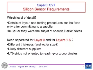
SuperB SVT Silicon Sensor Requirements Which level of detail? • Details of layout and testing procedures can be fixed only after committing to a supplier • In BaBar they were the subjet of specific BaBar Notes Keep separated for Layer 0 and for Layers 1-5 ? • Different thickness (and wafer size?) • Likely different suppliers • LY0 strips not oriented to read r-φ or z coordinates L. Bosisio - SuperB SVT Meeting - 21-02-2011
Silicon Sensor Requirements • General requirements: • Double-sided • Substrate thickness and tolerance • Orthogonal strips on the two sides • AC coupled (integrated decoupling capacitors) • Polysilicon bias resistors, connected to a metal Bias Line and located outside of an implanted Guard Ring (to minimize dead area) • N-side strips insulated by p-stops or p-spray ? • Geometrical requirements • Electrical requirements • Radiation tolerance • Testing procedures L. Bosisio - SuperB SVT Meeting - 21-02-2011
Geometrical requirements • Number of different sensor types (“Models”) • For each Model: • Overall dimensions • Dimensions of active area • Number and pitch of p-type strips • Number and pitch of n-type strips • Readout pitch on p-side • Readout pitch on n-side • Number and approx. locations of ‘AC’ bonding pads • Number and approx. locations of ‘DC’ probing pads L. Bosisio - SuperB SVT Meeting - 21-02-2011
Electrical requirements Many of these specs depend on model and side • Operating voltage range • Max. Guard Ring leakage current • Max. Bias Line current per unit (active) area • Max. leakage current of a single strip • Min. strip insulation resistance • Range of polysilicon bias resistance values • Max. interstrip capacitance per unit strip length • Min. AC coupling capacitance per unit strip length • Max. metal strip resistance per unit length • Stability requirements on leakage current, strip insulation and interstrip capacitance L. Bosisio - SuperB SVT Meeting - 21-02-2011
Radiation Tolerance Requirements Which kind/energy/amount of radiation should we specify? • Post-irradiation requirements (?): • Operating voltage range • Max. Guard Ring leakage current • Max. Bias Line current per unit (active) area • Max. leakage current of a single strip • Min. strip insulation resistance • Max. interstrip capacitance per unit strip length • Stability requirements on leakage current, strip insulation and interstrip capacitance L. Bosisio - SuperB SVT Meeting - 21-02-2011