
10 µm
Engineering Electron and Hole Transport in PbSe Nanowire Transistors Cherie Kagan , University of Pennsylvania, DMR 0805155.

10 µm
E N D
Presentation Transcript
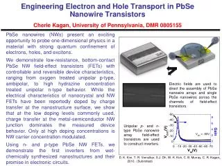
Engineering Electron and Hole Transport in PbSeNanowire TransistorsCherie Kagan, University of Pennsylvania, DMR 0805155 PbSenanowires (NWs) present an exciting opportunity to probe one-dimensional physics in a material with strong quantum confinement of electrons, holes, and excitons. We demonstrate low-resistance, bottom-contact PbSe NW field-effect transistors (FETs) with controllable and reversible device characteristics, ranging from oxygen treated unipolar p-type, ambipolar, to high hydrazine concentration treated unipolar n-type behavior. While the electrical characteristics of nanocrystal and NW FETs have been reportedly doped by charge transfer at the nanostructure surface, we show that at the low doping levels commonly used, charge transfer at the metal-semiconductor NW junction dominates the measured device behavior. Only at high doping concentrations is NW carrier concentration modulated. Using n- and p-type PbSe NW FETs, we demonstrate the first inverters from wet-chemically synthesized nanostructures and their promise in electronic circuits. Electric fields are used to direct the assembly of PbSenanowire arrays and single PbSenanowires across the channels of field-effect transistors. Unipolarp- and n-type PbSenanowire array field-effect transistors are used to construct inverters. • D. K. Kim, T. R. Vemulkar, S.J. Oh, W.-K. Koh, C. B. Murray, C. R. Kagan;, 2010. (Submitted) 10 µm
Measuring and Demonstrating the Behavior of Nanoscale MaterialsCherie Kagan, University of Pennsylvania, DMR 0805155 Graduate students from the Kagan group gave demonstrations on the physics of nanoscale materials to families visiting the Franklin Institute in Philadelphia for Nanoday. Undergraduate student TarunVemulkar worked over the summer and during the academic year with fellow graduate students to electrically probe charge transport in nanowire transistors. Controlling the nanowire environment impacts its measured transport characteristics. Graduate student David Kim describes magnetism in ferrofluids for Nanoday at the Franklin Institute Undergraduate student TarunVemulkar measuring nanowire devices in the nitrogen glove box