Milwaukee RF Radio Direction Finder System
The Milwaukee RF Radio Direction Finding System allows users to locate rockets and radio-controlled aircraft efficiently. The product comprises a two-part system where the receiver is held by the user, and the transmitter is placed into the rocket or aircraft. The system offers accurate locating within a 1-meter radius and can detect the transmitter from up to 1 km away. With a list price of $174.99 and a potential market size of $5,000,000, it targets males aged 8-70 worldwide in the recreation industry. The system's material and manufacturing costs are $50 each, with an annual volume projection of 50,000 units.


Milwaukee RF Radio Direction Finder System
E N D
Presentation Transcript
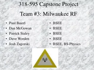
Milwaukee RF Daniel McGowan Lead Presentation Manager BSEE David Worden Lead Manufacturing Manager BSEE Josh Zagorski Lead Report Manager BSEE, BSPHY Paul Baierl Lead Project Integrator BSEE Patrick Staley Lead System Designer BSEE
Milwaukee RF Project • Radio Direction Finding System • Allow users to locate • Rockets • Radio-Controlled Aircraft • Two part system • Receiver is held by user • Transmitter is placed into rocket/aircraft Senior Design 318-595
No Competitors in Field Size of Market: $5,000,000 List Price of RDFS: $174.99 Market Geography: Worldwide Market Demography: Males ages 8 – 70 Market Industry: Recreation Material Cost: $50 Manufacturing Cost: $50 Annual Volume: 50,000 units Market Senior Design 318-595
Return on Investment Senior Design 318-595
Milwaukee RF Transmitter Signal Receiver Signal 500Hz Tone Locator Data Bus Antenna and Matching Network Transmitter Microprocessor and Display Vbat Tx LBO TX Receiver TX PS Vbat Rx LBO RX RX Power Supply Patrick Staley Dave Worden Paul Baierl Daniel McGowan Josh Zagorski Digital Power Analog Block Diagram Data Senior Design 318-595
Milwaukee RF Physical Layout Senior Design 318-595
Milwaukee RF Performance Requirements • Two antennas • Locate the transmitter beacon within 1 meter radius. • Detect transmitter from 1 km away Senior Design 318-595
Milwaukee RF Performance Requirements • User Interface • Digital display for location and distance. • LCD Display with Character Output to User. • 20 Characters by 2 rows • Accurate within 30 degrees. • Piezoelectric buzzer on beacon • 70 dB within 10 meters, pulsed tone every second. • Begins pulsed buzzer 15 minutes after turned on. Senior Design 318-595
Milwaukee RF Performance Requirements • User Interface Types • LCD Screen • Contrast Side Dial Control • Receiver On/Off Switch • Transmitter On/Off Switch • Transmitter Low Battery LED • Transmitter Buzzer Senior Design 318-595
Milwaukee RF Performance Requirements • Safety • TX I LIMIT MAX: 200 mA • TX GF ILIMIT MAX: 400 mA • RX 5V ILIMIT MAX: 400 mA • RX 5V GF ILIMIT MAX: 600 mA • RX 9V ILIMIT MAX: 200 mA • RX 9V GF ILIMIT MAX: 350 mA • Power Requirements • Transmitter: • 3V Li-Ion Battery • Capacity: 600 mAh • Min Life: 6 Hrs • Receiver • 3 x 3AA Battery EN91 • Capacity: 4500 mAh • Min Life: 24 Hrs Senior Design 318-595
Digital Signal Interface: VIH Min: 2.0 V VIL Max: 0.8V VOH Min: 2.4V VOL Max: 0.4 V IIH Max: 1 mA IIL Max: -1.6 mA IOH Max: -0.4 mA IOL Max: 16 mA Milwaukee RF Performance Requirements Senior Design 318-595
Analog Signal Interface: Voltage Range Input: 90 – 250 mV Input/Output Frequency Range 901.998 – 902.002 MHz Output Power TX Min: 20 mW Input Power RX Min: 75 μW SNR Output Min: 60 dB Input Impedance Min: 48 Ω Output Impedance Max: 52 Ω Note: Std. Antenna Impedance is 50 Ω Milwaukee RF Performance Requirements Senior Design 318-595
Milwaukee RF Standard Requirements • Environment and Safety • Operation Temperature Range: -10°C to 55°C • Operation Humidity Range: 0 to 100% • Non-condensing • Operation Altitude Range: -90 to 2500 Meters • Storage Temperature Range: -20°C to 60°C • Max Storage Duration: 2 years Senior Design 318-595
Milwaukee RF Standard Requirements • Power • Energy Source 1 (Transmitter) Min: • Battery 2 W • Energy Source 2 (Receiver) Min: • Battery 8 W • Operating Voltage Transmitter: • Tolerance: 4.875 – 5.125 V Min Ripple: 100 mV • Power Consumption Transmitter Max: 400 mAh • Operating Voltage Receiver: • Tolerance: 4.875 – 5.125 V Min Ripple: 100 mV • Tolerance: 8.775 – 9.225 V Min Ripple: 100 mV • Power Consumption Receiver Max: 1600 mAh Senior Design 318-595
Milwaukee RF Standard Requirements • Power • Transmitter Power Connector • 24mm Lithium Coin Battery Holder • PCB Mount • Receiver Power Connector • 3 AA Cell housing • PCB Mount Senior Design 318-595
Milwaukee RF Standard Requirements • Mechanical • Max Product Volume: 1750 cm3 • Shipping Container Size: 2000 cm3 • Maximum Product Mass: 3 kgs • Maximum Number of PCB: 2 • Maximum PCB Area: 225 cm2 • Maximum Shock Force: 30 G’s • Moisture Resistance: Sealed • Manufacturing • Maximum total parts count: 300 parts • Maximum unique parts count: 20 parts • Maximum parts and material cost: $50 • Maximum mfg. assembly/test cost: $50 • Max production lifetime: 10 years Senior Design 318-595
Milwaukee RF Block Diagram Description Senior Design 318-595
Milwaukee RF Safety Standards Standard • RoHS Component Compatibility • FCC Regulations • Section 15.245b • Fundamental f: 902-928 MHz • Field Strength of Fundamental • 500 mV/m • Field Strength of Harmonics • 1.6 mV/m • UL 2054 Standard for Commercial and Household Batteries • UL1642 Standard for Lithium Batteries Compliance Action • Select RoHS Compliant Parts • Comply with FCC antenna regulations • Comply with standard • Comply with standard Senior Design 318-595
Milwaukee RF Product Reliability • Failure rate at warranty period 4% • Reliability at warranty period 96% Senior Design 318-595
Transmitter Block Paul Baierl Senior Design 318-595
Transmitter Block Antenna - RDF Transmitter Microprocessor and Display Receiver TX PS RX Power Supply Senior Design 318-595
Transmitter Block Description • Purpose • Transmits a locator signal • Enables an audible buzzer after power up • Displays power status (on/off or low power) Senior Design 318-595
Performance Requirements • Power Input • 5 V supply • 4.875 – 5.125 V • 200 mA • 100 mV max voltage ripple Senior Design 318-595
Performance Requirements • Electrical Interfaces • Digital SignalInputs • 3V Logic Low Battery Input Senior Design 318-595
Performance Requirements • Electrical Interfaces • Analog Signal Outputs • 1 km Range of Signal • 9 dBm Minimum Output Power • 902 MHz Nominal Output Frequency • 100 kHz Bandwidth • 50 Ω Output Impedance Senior Design 318-595
Performance Requirements • User Inputs • None • Indicators and Displays • Flashing LED Power Indicator • LED Low Battery Indicator • Operation modes • ON/Off Senior Design 318-595
Performance Requirements • Mechanical Interfaces: • Molex connectors • 2 x WM4200 Connector • Connect LED and Buzzer to PCB • Mounting • Mounting Buzzer to Enclosure • M3 x 6 Phillips head screws • Connected Directly to Enclosure Senior Design 318-595
Performance Requirements • Safety Features Located on Power Supply • Reverse Voltage Protection • On/Off Switch • Over Current protection • Temperature Protection • Transmitter is Low Voltage Senior Design 318-595
Standard Requirements • Power Input • 5 VDC Supply • Tolerance: 4.875 – 5.125 V • Max. Ripple: 100 mV • Max. Current: 300 mA Senior Design 318-595
Standard Requirements • Environmental • Operating Temperature Range -10 to 55 ºC • Storage Temperature Range -20 to 60 ºC • Operating and Storage Humidity 0 to 100% N.C. • Operating Altitude Range -90 to 2500 meters • Maximum Shock Force 30 G • Maximum Shock Repetitions 100 • Manufacturing • Block Cost $11.80 • Parts Count 15 • Unique Parts Count 4 • Block Size 25 cm2 • Block Mass 40 grams • Block Volume 37.5 cm3 • Reliability (MTBF) 46 Years Senior Design 318-595
Standard Requirements • Allocations Allowed Actual • Cost 23% 23.6% • Parts 7% 6% • Unique Parts 7% 5% • Power Consumption 90% 30% • Mass 4% 1% • PCB Area 10% 11% • Volume 16% 2% Senior Design 318-595
Standard Requirements • EMC Standards • IEC 61000-4-2 • Electrostatic Discharge • IEC 61000-4-6 • Electromagnetic disturbances coming from RF transmitters Senior Design 318-595
Standard Requirements • Reliability • Product Lifetime: 10 years Senior Design 318-595
Input/Output • Inputs • 5 V supply • 4.875 – 5.125 V • 200 mA • 100 mV maximum voltage ripple • 3 V Logic Low Battery Signal • VIH = 2 – 3 Volts • VIL = 0 – 0.8 Volts Senior Design 318-595
Input/Output • Outputs • 902 MHz Analog output signal • 100 kHz bandwidth • 12 dBm Power Output • 50 Ω output resistance Senior Design 318-595
Transmitter Block Diagram LBO TX Microcontroller +5 VDC Alarm Transmit Locator Signal HB Signal Buzzer Power Sensing & Low Voltage LED Transmitter Digital Signals Analog Locator Signal Power Senior Design 318-595
Prototype Schematic Senior Design 318-595
Design Calculations Voltage Divider Equation Output Impedance Matching Equations Senior Design 318-595
Theory of Operation • A VCO is supplied with the correct tuning voltage allowing it to transmit a 902 MHz sine wave. • A microcontroller will modulate the 902 MHz signal, display power status, and enable and audible buzzer a predetermined time after power up. Senior Design 318-595
Component Selection • Why did we choose the Mini-Circuits voltage controlled oscillator POS – 1060? • Team members had previous experience with this device • Output frequency was easily selected using the supply voltage • Hermetically sealed • Greatly reduced the number of components Senior Design 318-595
Component Selection • Why did we choose the PIC16F628? • Team member had previous experience with the device • Had access to the equipment needed to program the chip • The device is easy to use and program Senior Design 318-595
Theory of Operation • Choosing the Trasmitter • 902 MHz analog signal • Small size • Light weight • Easily tunable • Mini-Circuits POS-1060 • 750 – 1060 MHz • 18 – 32 MHz/V • Reduced number of parts • Easily tuned using Voltage Senior Design 318-595
Component Selection • POS - 1060 Senior Design 318-595
Theory of Operation • Choosing the Microcontroller • Small size • Light weight • Easy to program • PIC16F628 • SOIC package • External Clock • Access to programmer • Previous experience with • device Senior Design 318-595
Component Selection • PIC16F628 • Total Power Dissipation 800 mW • External 22MHz clock crystal Senior Design 318-595
Design Calculations Choosing Bypass Capacitors • Standard 0.1μF ± 10%, 6.3V Ceramic • For microcontroller and MOSFET • All other capacitors ± 10%, 6.3V Ceramic • Size chosen depending discharge times • needed (long or short) Choosing Resistor Values • Standard 10 kΩ ±1%, 1/8 W • Chosen to limit current into • microcontroller Senior Design 318-595
Prototype BOM Senior Design 318-595
Prototype Netlist Senior Design 318-595
Production Schematic Senior Design 318-595