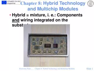
Chapter 8: Hybrid Technology and Multichip Modules
Chapter 8: Hybrid Technology and Multichip Modules. Hybrid = mixture, i. e.: Components and wiring integrated on the substrate. Types of Hybrids and Multichip Modules. Thick film technology High temperature thick film hybrid technology Polymer thick film hybrid technology

Chapter 8: Hybrid Technology and Multichip Modules
E N D
Presentation Transcript
Chapter 8: Hybrid Technology and Multichip Modules • Hybrid = mixture, i. e.: Components and wiring integrated on the substrate Electronic Pack….. Chapter 8: Hybrid Technology and Multichip Modules
Types of Hybrids and Multichip Modules • Thick film technology • High temperature thick film hybrid technology • Polymer thick film hybrid technology • Thin film technology • Conventional thin film technology (one conductor layer) • Multilayer thin film technology • Multichip modules: • Multilayer ceramic (MCM-C) (C for ceramic) • Multilayer thin film (MCM-D) (D for deposited) • Multilayer fineline circuit boards (MCM-L) (L for laminated) Please also confer to Chapter 5. Electronic Pack….. Chapter 8: Hybrid Technology and Multichip Modules
High Temperature Thick Film Technology • Important substrate properties • Dimensional stability • Good adhesion • High thermal conductivity • Thermal compatibility with components • High electrical resistivity • Low dielectric constant (not satisfied in alumina) • Low dielectric loss tangent • Good machinability (not satisfied in ceramics) • Low price Electronic Pack….. Chapter 8: Hybrid Technology and Multichip Modules
High Temp Thick Film, continued • Practical materials • Alumina • Aluminium nitride • (Beryllia) • (Silicon carbide) Table 8.1:Properties of substrate materials for hybrid technology.P: Plastic In: Insulator Electronic Pack….. Chapter 8: Hybrid Technology and Multichip Modules
Conductor Materials • Composition • Functional element (metal paticles) • Binder (glass particles) • Solvents • Desired properties • High electrical conductivity • Good adhesion to substrate • Good solderability • Good bondability • Low price Electronic Pack….. Chapter 8: Hybrid Technology and Multichip Modules
Conductor Materials, continued • Practical functional element • Gold • Ag/Pd • Ag/Pt • Copper Table 8.2 Properties of thick film conductor systems Electronic Pack….. Chapter 8: Hybrid Technology and Multichip Modules
Thick Film Resistors • Important properties • Large range of resistor values • High stability • Low thermal coefficient of resistivity • Low voltage coefficient of resistivity • Low noise • Materials • Oxides of ruthenium • Oxides of iridium, rhodium, osmium • Sheet resistance: 1 - 109 ohms/sq Electronic Pack….. Chapter 8: Hybrid Technology and Multichip Modules
Properties of Thick Film Resistors Table 8.3: Typical properties of thick film resistors. Electronic Pack….. Chapter 8: Hybrid Technology and Multichip Modules
Termination of Thick Film Resistors Fig. 8.2: Thick film resistor with termination Electronic Pack….. Chapter 8: Hybrid Technology and Multichip Modules
Insulators / Dielectrics • Desired properties: • High insulation resistance • High breakdown field • Low dielectric constant (insulation) • Suitable/high dielectric constant (dielectric) • Low temperature coefficient (dielectric) • Low voltage coefficient (dielectric) • Low loss tangent • Little porosity Electronic Pack….. Chapter 8: Hybrid Technology and Multichip Modules
Insulators / Dielectrics, continued • Materials • Aluminium oxide/glass (insulator) • Ceramics/glasses as for capacitors (dielectric) • Please also see Chapter 4 Electronic Pack….. Chapter 8: Hybrid Technology and Multichip Modules
Insulators / Dielectrics, continued Table 8.4: Typical properties of printed and discrete capacitors. Electronic Pack….. Chapter 8: Hybrid Technology and Multichip Modules
Production Process for High Temperature Thick Film Technology • Layout and photolithographics • CAD work • Photo or laser plotting of master films • Printing screens made with master films Electronic Pack….. Chapter 8: Hybrid Technology and Multichip Modules
Production process, continued • Printing process • Printing • Drying at 100 - 150 °C • Firing at 700 - 1000 °C Fig 8.1: Typicaltemperature profilefor thick filmfiring. Electronic Pack….. Chapter 8: Hybrid Technology and Multichip Modules
Production process, continued • Testing and laser trimming • Initial value targeted 20 - 30 % below specified value • Laser trimming to increase resistance within ± 0.5 or ± 1.0 % Fig. 8.4: Probe card for testing of thick- and thin film hybrid circuits. Coaxial probes are used for high frequency signals. Electronic Pack….. Chapter 8: Hybrid Technology and Multichip Modules
Laser trimming Fig. 8.5: Laser trim cut forms: a): L-cut, the most common b): Top hat plunge cut c): Digital trimming, which is most used for high precision thin film resistors a) b) c) Electronic Pack….. Chapter 8: Hybrid Technology and Multichip Modules
Laser trimming, continued Fig. 8.6: Laser trimmer for thick film hybrid circuits, ESI Model 44. Electronic Pack….. Chapter 8: Hybrid Technology and Multichip Modules
Production process, continued Fig. 8.7: Process flow for mounting of thick film hybrid circuits based on: a): Naked ICs and gluing of discrete components. Electronic Pack….. Chapter 8: Hybrid Technology and Multichip Modules
Production process, continued Fig. 8.7: Process flow for mounting of thick film hybrid circuits based on: b): Soldering of packaged ICs and discrete components. Electronic Pack….. Chapter 8: Hybrid Technology and Multichip Modules
Polymer Thick Film Technology • In polymer thick film hybrid technology (PTF) conductors, resistors and insulating layers use a polymer matrix instead of glass matrix, and these are made in several layers on ordinary printed wiring board laminates, flexible substrates and injection moulded plastic materials that can serve as combined printed circuits and chassis. Electronic Pack….. Chapter 8: Hybrid Technology and Multichip Modules
Polymer Thick Film, continued • Advantages • Low price • Simple processes • Fast production throughput • Well suited for repair/modification • Printed resistors possible • Additive technology • Printed wiring boards for substrates • Specialities: • Membrane switch panels • Contacts Electronic Pack….. Chapter 8: Hybrid Technology and Multichip Modules
Polymer Thick Film, continued • Limitations • Satisfies only moderate environmental requirements • Low/moderate complexity • High sheet resistivity in conductors • Special design rules • Limited solderability • Limited shelf life for pastes • Limited availability Electronic Pack….. Chapter 8: Hybrid Technology and Multichip Modules
Polymer Thick Film, continued Fig. 8.8: Polymer Thick film (PTF) carbon technology, for: a): Keyboard contacts. b): Contacts of LCD- displays. c): Sliding potentiometer. CPTF means carbon type PTF. Electronic Pack….. Chapter 8: Hybrid Technology and Multichip Modules
Polymer Thick Film, continued • Materials • Matrix: Thermosetting /thermoplastic polymer • Conductor: Ag, Cu, C • Solvents • Additives to adjust consistency • Ceramic or other additives Electronic Pack….. Chapter 8: Hybrid Technology and Multichip Modules
Polymer Thick Film, continued • A typical process • The starting material is a laminate with a single sided etched conductor pattern in Cu foil • 1. Cleaning of the board • 2. Printing of PTF insulation layer, 2 prints, drying in between • 3. Drying • 4. UV curing • 5. Printing of PTF conductor • 6. Drying • 7. Curing in IR in-line furnace • 8. Chemical plating of metal (Optional) • 9. Printing of top layer • 10. Drying • 11. Curing in IR furnace. Electronic Pack….. Chapter 8: Hybrid Technology and Multichip Modules
Polymer Thick Film, continued Fig. 8.9: Membrane switch panel, principle. Electronic Pack….. Chapter 8: Hybrid Technology and Multichip Modules
PTF, continued Fig. 8.10: PTF based printed wiring boards: a): Single sided board with PTF for one complete conductor layer on top of one Cu foil conductor plate. b): Double sided, through hole plated board with one extra PTF conductor layer on each side. c): Double sided board through hole printed PTF conductor, instead of through hole plating.d): PTF resistor Electronic Pack….. Chapter 8: Hybrid Technology and Multichip Modules
Thin Film Technology • Substrate materials • Alumina, glass, silicon • Conductor materials • Gold, aluminium • Resistor materials • NiCr (Chromnickel), Ta2N (Tantalnitrid) • Insulation/dielectrics/passivation materials • SiO2 (Silicon dioxide), SiN3 (Silicon nitride), Al2O3 (Silicon nitride), Ta2O5 (Tantaloxide) Electronic Pack….. Chapter 8: Hybrid Technology and Multichip Modules
Thin Film Technology, continued Table 8.5: Properties of thin film resistors. (d: skin depth. Evap: Vacuum evaporation. Sp: Sputtering) Electronic Pack….. Chapter 8: Hybrid Technology and Multichip Modules
Thin FilmProcessing • Photolithography and etching • Vacuum evaporation • Sputtering • Plating • Oxidation Fig. 8.11: Process flow for production of thin film hybrid circuits. Electronic Pack….. Chapter 8: Hybrid Technology and Multichip Modules
Thin Film Processing, continued Fig. 8.12 : Structure of thin film resistor with gold termination. Electronic Pack….. Chapter 8: Hybrid Technology and Multichip Modules
Thin Film Processing, continued Fig. 8.13: Thin film microwave circuit, schematically. Electronic Pack….. Chapter 8: Hybrid Technology and Multichip Modules
Thin Film Processing, continued Fig. 8.14: Thin film transistors, structure. Electronic Pack….. Chapter 8: Hybrid Technology and Multichip Modules
Thin Film Processing, continued • Circuit production • Glueing • Wire bonding • Testing • Packaging in hermetic (metal) box Electronic Pack….. Chapter 8: Hybrid Technology and Multichip Modules
Multilayer Thin Film - MCM-D • Process • 1. Spinning polyimide insulation • 2. Deposition Al metallization • 3. Photolithography, wet etch • 4. Spinning polyimide • 5. Etching vias • 6. Repetition steps 1 - 5 • 7. Metallization and etching of metal Electronic Pack….. Chapter 8: Hybrid Technology and Multichip Modules
MCM-D, continued Fig. 8.15 a): AT&T´s structure for multilayer thin film. Please also see also Figure 2.13. Electronic Pack….. Chapter 8: Hybrid Technology and Multichip Modules
MCM-D, continued Fig. 8.15 b): Cross section of Raychem´s High Density Interconnect (HDI) schematically and observed through microscope. Electronic Pack….. Chapter 8: Hybrid Technology and Multichip Modules
MCM-D, continued Fig. 8.16: Elements of the design rules for Raychem´s HDI technology Electronic Pack….. Chapter 8: Hybrid Technology and Multichip Modules
MCM-D, continued Fig. 8.17: Characteristic impedance for Raychem´s HDI as function of the ratio between conductors width and dielectric thickness. Electronic Pack….. Chapter 8: Hybrid Technology and Multichip Modules
MCM-D, continued Fig. 8.18a): Dissipation factor for Raychem´s HDI Electronic Pack….. Chapter 8: Hybrid Technology and Multichip Modules
MCM-D, continued Fig. 8.18. b):Typical attenuation, as function of frequency, for Raychem´s HDI. Even at 10 GHz attenuation in the conductor metal dominates. Electronic Pack….. Chapter 8: Hybrid Technology and Multichip Modules
MCM-D, continued • Advantages • Optimal thermal match when Si substrate • High thermal conductivity in Si: 150 W/°C x m • Termination resistors and decoupling capacitors integrated in substrate • Compatibility with: • Wire bonding • TAB • Flip chip • Very high conductor density/package density • Very good high frequency properties • Good mechanical properties of Si substrate • High reliability Electronic Pack….. Chapter 8: Hybrid Technology and Multichip Modules
MCM-D, continued • Disadvantages: • Low availability and high cost • Polyimide is hygroscopic • Important properties change • Reliability problems • Hermetic encapsulation necessary • Immature technology Electronic Pack….. Chapter 8: Hybrid Technology and Multichip Modules
Multilayer Ceramic Modules - MCM-C • Materials • Alumina • Aluminium nitride • Pioneer: IBM • Fabrication: Green Tape process Electronic Pack….. Chapter 8: Hybrid Technology and Multichip Modules
MCM-C, continued Fig. 8.19: Production process for multilayer ceramic, schematically. Electronic Pack….. Chapter 8: Hybrid Technology and Multichip Modules
MCM-C, continued • Advantages • High thermal conductivity • Low TCE, match to Si, GaAs, SMDs • Compatible to flip chip, wire bonding, TAB, SMD soldering • Control over characteristic impedance • Hermetic encapsulation possible, high reliability • Many conductor layers, high yield • Edge contacts, etc. brazed on Electronic Pack….. Chapter 8: Hybrid Technology and Multichip Modules
MCM-C, continued • Disadvantages • Low electrical conductivity in inner layers (Rsq ≈ 15 mOhm/sq) • High dielectric constant, r ≈ 9 - 10 • High startup cost for custom specific circuits Electronic Pack….. Chapter 8: Hybrid Technology and Multichip Modules
MCM-C, continued Fig. 8.20: Combination of naked chips in cavities and soldered, packaged SMD components on multilayer ceramic module Electronic Pack….. Chapter 8: Hybrid Technology and Multichip Modules
MCM-C, continued Fig. 8.21.a: Characteristic impedance for typical geometries and dimensions, Al2O3-based multilayer ceramic: a): Open microstrip. Electronic Pack….. Chapter 8: Hybrid Technology and Multichip Modules
MCM-C, continued Fig. 8.21.b: Characteristic impedance for typical geometries and dimensions, Al2O3-based multilayer ceramic: b): Buried microstrip. Electronic Pack….. Chapter 8: Hybrid Technology and Multichip Modules