THIN FILM DEPOSITION – Chapter 9 Introduction
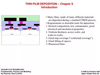
THIN FILM DEPOSITION – Chapter 9 Introduction. • Many films, made of many different materials are deposited during a standard CMOS process. • Requirements or desirable traits for deposition: 1. Desired composition, low contaminates, good electrical and mechanical properties.

THIN FILM DEPOSITION – Chapter 9 Introduction
E N D
Presentation Transcript
THIN FILM DEPOSITION – Chapter 9 Introduction • Many films, made of many different materials are deposited during a standard CMOS process. • Requirements or desirable traits for deposition: 1. Desired composition, low contaminates, good electrical and mechanical properties. 2. Uniform thickness across wafer, and wafer-to-wafer. 3. Good step coverage (“conformal coverage”). 4. Good filling of spaces. 5. Planarized films . SILICON VLSI TECHNOLOGY Fundamentals, Practice and Modeling By Plummer, Deal & Griffin © 2000 by Prentice Hall Upper Saddle River NJ
• Note the aspect ratios and the need for new materials. • Note also the number of metal layers requiring more deposition steps. SILICON VLSI TECHNOLOGY Fundamentals, Practice and Modeling By Plummer, Deal & Griffin © 2000 by Prentice Hall Upper Saddle River NJ
Thin Film Deposition • Quality – composition, defect density, mechanical and electrical properties • Uniformity – affect performance (mechanical , electrical) Thinning leads to R Voids: Trap chemicals lead to cracks (dielectric) large contact resistance and sheet resistance (metallization) AR (aspect ratio) = h/w with feature size in ICs.
Examples Poor step coverage with increasing AR Thinning causes metal resistance to increase, generates heat and lead to failure
Chemical Vapor Deposition Methods of Deposition: Chemical Vapor Deposition (CVD):APCD, LPCVD, HDPCVD Physical Vapor Deposition (PVD: evaporation, sputtering) Cold wall reactor Atmospheric Pressure : APCVD Cold wall reactors (walls not heated - only the susceptor) Flat on the susceptor Low pressure: LPCVD – batch processing. Hot wall reactor
Atmospheric Pressure Chemical Vapor Deposition Steps in deposition Transport by forced convection Transport of byproducts by forced convection @ the surface (4): decomposition, reaction, surface migration attachment etc. By diffusion through boundary layer Diffusion through the B. L Desorption of by products adsorption (3) May be desorption which depends on a sticking coefficient (4) Growth rate for Si deposition N=5•1022cm-3 transport Mole fraction of the incorporating species in the gas phase. reaction Partial pressure Steady state As in Deal-Grove model for oxidation • V = 0.14 m/min PG @ 1 torr Ptotal = 1 atm = 760 torr Total concentration in the gas phase CT = 1 * 1019 cm-3 5 * 1022
Growth Kinetics Determined by the Smaller of ks or hG Two limiting cases 1) Surface reaction ks << hG Control: fast transport slow reaction kS limited deposition is VERY temp sensitive. hG limited deposition is VERY geometry (boundary layer) sensitive Limited by transport 2) Mass transfer or gas phase diffusion hG << ks Temperature uniformity more important than the gas flow wafers vertically poly-Si Put wafers flat to ensure flow uniformity @ the Si surface. Epitaxy Fast reaction and slow transport. Both are linear with time (t) Light mass APCVD SiO2 heavy (111) Si shows slower v – fewer attachment sites than in (100) Si SiH4 the fastest growth Ea 1.6 eV for all Si sources H desorption from the Si surface. With H2 as a gas carrier
Boundary Layer – Diffusion to the Surface Gas moves with the constant velocity U. Boundary layer (caused by friction ) increases along the susceptor, mass transfer coefficient hG decreases, gas depletion caused by consumption of the reacting species (concentrations decrease) Growth rate decreases along the chamber • Use tilted susceptor • Use T gradient 5-25°C • Gas injectors along the tube • Use moving belt viscosity B.L. Deposition of alloys DIFFICULT – various reactions, kinetics (species, precursors) Use PVD rather than CVD gas density
Doping in CVD for EPITAXY Intentional and Unintentional • The dopant sources at the surface go through: • dissociation of hydride gas • lattice site incorporation • burying of dopants by other atoms in the film Autodoping: 1 - 4 Si source + Dopant (AsH3, PH3, or B2H6) Simulation very inaccurate : chamber design etc. In deposition , the doping, 800-1000°C outdiffusion autodoping outdiffusion T&time of CVD autodoping The growth is faster than the diffusion Calculate all distributions (=contributions) to get C(x,t)
Low Pressure Chemical Vapor Deposition Operate at the surface reaction limited regime lower deposition temperatures Larger diffusion @ lower P DG1/Ptotal low pressure hG increases ~ 100 X for 760 torr 1 torr transport less important Surface reaction controls the growth • LPCVD reactors use • Vertical wafer stacking • P = 0.25 – 2.0 torr • T = 300 – 900 °C ( + 1 °C) temperature gradient increase 5 – 25% to compensate reactants depletion distributed feeding. • Less autodoping (at lower P) • Fewer particulates. • Possible disadvantages: • Deposition rates may be too low, Film quality decreases • Shadowing (less gas-phase collisions) due to directional diffusion to the surface deterioration of the step coverage and filling.
Plasma Enhanced Chemical Vapor Deposition(PECVD) • Used when : • Low T required (dielectrics on Al, metals) but CVD at decreased T gives increased porosity, poor step coverage. • Good quality films – energy supplied by plasma increases film density, composition, step coverage for metal decreases but WATCH for damage and by product incorporation. 13.56 MHz P 50 mtorr - 5 torr Plasma: ionized excited molecules, neutrals, fragments, ex. free radicals very reactive reactions @ the Si surface enhanced increase deposition rates Ions, electrons, neutrals = bombardment Outgassing , peeling , cracking stress. 200- 350 °C • High Density Plasma CVD dense layers ( SiO2) at low T (150 °C) and low P ( 1- 10 m torr); T increases to 400°C by bombardment • Separate RF (gives substrate biasing bombardment) from plasma generation (Electron Cynclotron resonance ECR and Inductively coupled Plasma ICP) • Controlled bombardment (angular -> sputtering) preferential sputtering of sloped surface improved planarization and filling
High Density Plasma (HDP) CVD • Remote high density plasma with independent RF substrate bias. • Allows simultaneous deposition and sputtering for better planarization and void-free films (later). • Mostly used for SiO2 deposition in backend processes. SILICON VLSI TECHNOLOGY Fundamentals, Practice and Modeling By Plummer, Deal & Griffin © 2000 by Prentice Hall Upper Saddle River NJ
Physical Vapor Deposition (PVD) – no chemical reactions (except for reactive sputtering) Evaporation • Advantages: • Little damage • Pure layers (high vacuum) • Disadvantages: • Not for low vapor pressure metals • No in-situ cleaning • Poor step coverage Very low pressure (P < 10 –5 torr) - long mean free path. • purer – no filaments, only surface of the source melted • X-rays generated trapped charges in the gate oxides anneal it !
Evaporation Deposition rates: Ideal cosine emission Wafer holders to increase uniformity of deposition Use spherical holders & rotate them in a planetary configuration Projected area The largest flux for the perpendicular direction Practical cases Knudsen –cell like behavior Affected by a crucible (melt,) nonuniform deposition l r and cos k v Emitted fluxes from crucibles source here is || to the wafer lower because of cosi emission
Evaporation Partial Pressure (Pe) of the source (target) No alloys – partial pressure differences 1-10 mtorr Needed for reasonable v 0.1 - 1m/min Use separate sources and e-beam • Step Coverage Poor : • Long mean free path (arrival angle not wide = small scattering) and low T (low energy of ad-atoms) • Sticking coefficient high (@ T) no desorption and readsorption poor step coverage • Heating can increase Sc but may change film properties (composition, structure) Deposition Sticking coefficient Rarely used in IC fabrication
Sputter Deposition Higher pressures 1 –100 mtorr ( < 10-5 torr in evaporation) -> contaminations! Use ultra clean gasses and ultra clean targets Major Technique in Microelectronics for: DC Sputtering (for metal) • Alloys (TiW, TiN etc) • good step coverage • controlled properties Conductive Al, W, Ti Ar inert gas at low pressure. No free radicals formed by Ar (ex. O, H ,F as was for PECVD)
DC Sputtering Low concentrations of electrons -> few collisions -> large voltage here 0.1 –10 mm e- The source of material to be deposited I+ low e--conc. e- collide with Ar atoms excitation=glow Conductive ! Ar ions (+) strike the target and sputter ions electrons do not have high energy yet dark glow anode sheath. (Crookes dark space) ions positive potential (form next to each surface = anode) I+ and e- strike the surface: µe larger (smaller mass than for ions) more electrons than ions E field due to charge imbalance Vp (10 V develops) to decrease e- accumulation + potential Ions get neutralized by e- and diffuse to the wafer surface secondary electrons! They sustain the plasma Very small sputtering at the anode can be used for bias sputtering and ionized sputtering
Sputtering Cathode DC Sputtering CONDUCTOR secondary electrons 10-20 eV electrons sustain the plasma - ionization of the gas Can be incorporated in the film desorption (small) Bombardment by I+ , e- charges and neutrals adsorption WAFERS migration heating can be used in hot sputter reflow Reactive Sputter Deposition = add gas: . N2 Ti N . O2 Ti O2
SPUTTERING YIELD much smaller differences in sputtering yields then in partial pressures of components (target) in evaporation Neutral + Target gas Target atom Effect of mass (gas) & Energy TiW steady state sputtering Effect of mass (target) implantation
RF Sputter Deposition Dielectric Instead of DC: 13.6 MHz RF coupled capacitively to plasma DC sputter cannot be used for dielectrics secondary e- plasma extinguished (VZ ) in 1-10µs e- charge on electrode (e- are fast so they keep up with RF) More e- on the walls - charge built-up potential VP potential @ the target ( area) faster, smaller tenths of volts A1 A2 several 100V wafers For A1=A2 Ions would bombard the target and the deposited layer V1/V2=(A2/A1)m m=1-2 = NON-CONDUCTING A2 Oscillating (with RF) e- ionization yield pressure can be used large A1area + magnet e- trajectory Magnetron Sputter Deposition have better ionization yields deposition rates (10-100X) better film quality (Ar needed) use in DC & RF ( heating of the target since I+ )
BIAS SPUTTERING - Small(-) Bias @ the Wafer Chuck 50 – 300V on wafers 700 – 2000V on target • For : • precleaning = sputter etch • better planarity step coverage • properties (stress, compos.) Not used much particulates from flaking Use High Density Plasma CVD instead or Collimated Sputtering and Ionized Sputtering Wider arrival small in extended sources = not point sources evap; in point sources Collimate the beam by using holes to direct the ions to the wafers : that u
Ionized Sputter Deposition or HDP Sputtering • In some systems the depositing atoms themselves are ionized. An RF coil around the plasma induces collisions in the plasma creating the ions (50-85% ionized). Highly directional flux Better solution than a collimator (holes) • This provides a narrow distribution of arrival angles which may be useful when filling or coating the bottom of deep contact hole. SILICON VLSI TECHNOLOGY Fundamentals, Practice and Modeling By Plummer, Deal & Griffin © 2000 by Prentice Hall Upper Saddle River NJ
VARIOUS DEPOSITION TECHNIQUES • mass transfer regime • T oxide evaporation • Cl- cleaning (HCL etc) 0.5 – 2 torr 80 – 200 torr ! VLSI Low T: -Si instead of poly_Si give better step coverage than sputtering • & better doping control • Selectivity with Cl, poor for SiHCL Conditions: density of SiO2, step coverage, contaminations (C, H, N) all that determines T, pressure and gas used. TEOS porous BPSG 4-8% B, P) reflow for planarization, steam, N2 LPCVD (conformal, 650-800°C) Barrier ! Al – TIBA or DMAH Al-H C - better r Cu or Al-Cu sputtered on CVD Al diffusion @ 400 0C plugs = salicide 400 – 7000C
Polysilicon @ low T amorphous Si As, P segregate @ the grain boundaries r ( B does not ! ) columnar structure 625 °C As & P deposition rate of poly – Si use doping after poly deposition B Vpoly - Si
Models and Simulation • Within the past decade, a number of simulation tools have been developed for topography simulation. • Generalized picture of fluxes involved in deposition. (No gas phase boundary layer is included, so this picture doesn't fully model APCVD.) • Essentially the same picture will be used for etching simulation (in Chapter 10). (14) • To simulate these processes, we need mathematical descriptions of the various fluxes. • Modeling specific systems involves figuring out which of these fluxes needs to be included. SILICON VLSI TECHNOLOGY Fundamentals, Practice and Modeling By Plummer, Deal & Griffin © 2000 by Prentice Hall Upper Saddle River NJ
• Finally, ions striking the surface can sometime enhance the deposition rate (by supplying the energy to drive chemical reactions for example), so that (22) LPCVD Deposition Systems • In these systems there are no ions involved and hence no sputtering. Surface diffusion also is usually not important. SILICON VLSI TECHNOLOGY Fundamentals, Practice and Modeling By Plummer, Deal & Griffin © 2000 by Prentice Hall Upper Saddle River NJ
PECVD Deposition Systems • In these systems an ion flux can enhance the deposition rate by changing the surface reactions. Sputtering is usually not significant because the ion energy is low, nor is direct deposition of ions significant. (25) • Thus where Kd and KI are relative rate constants for the neutral and ion-enhanced components respectively. SILICON VLSI TECHNOLOGY Fundamentals, Practice and Modeling By Plummer, Deal & Griffin © 2000 by Prentice Hall Upper Saddle River NJ
Ionized PVD Deposition Systems • These systems are complex to model because both ions and neutrals play a role. • They are often used for metal deposition so that Ar+ ions in addition to Al+ or Ti+ ions may be present. • Thus almost all the possible terms are included where Fd includes the direct and redeposited (emitted) neutral fluxes, Fi includes the direct and ion-induced fluxes associated with the ions, and Frd models redeposition due to sputtering. SILICON VLSI TECHNOLOGY Fundamentals, Practice and Modeling By Plummer, Deal & Griffin © 2000 by Prentice Hall Upper Saddle River NJ
High Density Plasma CVD Deposition Systems • Very similar to IPVD (except neutral direct flux not as important): (29) SILICON VLSI TECHNOLOGY Fundamentals, Practice and Modeling By Plummer, Deal & Griffin © 2000 by Prentice Hall Upper Saddle River NJ
Models in SPEEDIE LPCVD: PECVD: Standard PVD: High T PVD: Ionized PVD: HDP CVD: SILICON VLSI TECHNOLOGY Fundamentals, Practice and Modeling By Plummer, Deal & Griffin © 2000 by Prentice Hall Upper Saddle River NJ
SILICON VLSI TECHNOLOGY Fundamentals, Practice and Modeling By Plummer, Deal & Griffin © 2000 by Prentice Hall Upper Saddle River NJ
J.P. McVittie, J.C. Rey, L.Y. Cheng, and K.C. Saraswat, "LPCVD Profile Simulation Using a Re-Emmission Model", IEDM Tech. Digest, 917-919 (1990). L-Y. Cheng, J. P. McVittie and K. C. Saraswat, " Role of Sticking Coefficient on the Deposition Profiles of CVD Oxide, "Appl. Phys. Lett., 58(19), 2147-2149 (1991). SILICON VLSI TECHNOLOGY Fundamentals, Practice and Modeling By Plummer, Deal & Griffin © 2000 by Prentice Hall Upper Saddle River NJ
PECVD LPCVD J.P. McVittie, “Test Structure and Modeling Studies of Deposition and Etch Mechanisms”, Talk TC1-WeM6, AVS mtg in Orlando, Florida, 1993 SILICON VLSI TECHNOLOGY Fundamentals, Practice and Modeling By Plummer, Deal & Griffin © 2000 by Prentice Hall Upper Saddle River NJ
Parameter Values for Specific Systems • • PVD systems - more vertical arrival angle distribution (low pressure line of sight • or field driven ions). n > 1 typically. • • CVD systems provide isotropic arrival angle distributions (higher pressure, • gas phase collisions, mostly neutral molecules). n ≈ 1 typically. • • PVD systems usually provide Sc of 1. Little surface chemistry involved. Atoms • arrive and stick. • • CVD systems involve surface chemistry and Sc <<1. Molecules often reemit and • redeposit elsewhere before reacting. • CVD systems provide more conformal deposition. SILICON VLSI TECHNOLOGY Fundamentals, Practice and Modeling By Plummer, Deal & Griffin © 2000 by Prentice Hall Upper Saddle River NJ
Topography Simulation (Using SPEEDIE) • SPEEDIE simulations for LPCVD deposition of SiO2 with Sc = 1 (which is more typical of PVD than LPCVD) and varying values of n, the arrival angle distribution factor: (a) n=1; (c) n=10. • Worse step coverage results as n increases (the arrival angle distribution narrows). • Even for n = 1, conformal coverage is not achieved. • SPEEDIE simulations for LPCVD deposition of SiO2 in a narrow trench with the same isotropic arrival angle distribution (n=1) but different values of Sc: (a) Sc = 1; (b) Sc = 0.1; and (c) Sc = 0.01. • Reducing Sc is much more effective than changing n if conformal deposition is desired. SILICON VLSI TECHNOLOGY Fundamentals, Practice and Modeling By Plummer, Deal & Griffin © 2000 by Prentice Hall Upper Saddle River NJ
Simulations - CVD • Results of SPEEDIE LPCVD simulations with the sidewall angle changed. Sc = 0.2 and n = 1. Note the improved trench filling. 90˚ 85˚ 80˚ • SPEEDIE simulations comparing LPCVD and HDPCVD depositions. (a) LPCVD deposition of SiO2 over rectangular line. Sc = 0.1 and n = 1. (b) HDPCVD deposition, with directed ionic flux and angle-dependent sputtering, over rectangular line showing much more planar topography. • CMP might still be required in the HDPCVD case to fully planarize the surface. SILICON VLSI TECHNOLOGY Fundamentals, Practice and Modeling By Plummer, Deal & Griffin © 2000 by Prentice Hall Upper Saddle River NJ
Simulations - CVD • SPEEDIE simulations comparing LPCVD and HDPCVD depositions. (c) LPCVD deposition in trench, showing void formation. Sc = 0.2 and n = 1. (d) HDPCVD deposition in trench, showing much better filling. • HDPCVD has a strong directed ion component and any overhangs that form are sputtered away. • Actual SEM images of HDP oxide deposition. SILICON VLSI TECHNOLOGY Fundamentals, Practice and Modeling By Plummer, Deal & Griffin © 2000 by Prentice Hall Upper Saddle River NJ
Summary of Key Ideas • Thin film deposition is a key technology in modern IC fabrication. • Topography coverage issues and filling issues are very important, especially as geometries continue to decrease. • CVD and PVD are the two principal deposition techniques. • CVD systems generally operate at elevated temperatures and depend on chemical reactions. • In general either mass transport of reactants to the surface or surface reactions can limit the deposition rate in CVD systems. • In low pressure CVD systems, mass transport is usually not rate limiting. • However even in low pressure systems, shadowing by surface topography can be important. • In PVD systems arrival angle distribution is very important in determining surface coverage. Shadowing can be very important. • A wide variety of systems are used in manufacturing for depositing specific thin films. • Advanced simulation tools are becoming available, which are very useful in predicting topographic issues. • Generally these simulators are based on physical models of mass transport and surface reactions and utilize parameters like arrival angle and sticking coefficients from direct and indirect fluxes to model local deposition rates. SILICON VLSI TECHNOLOGY Fundamentals, Practice and Modeling By Plummer, Deal & Griffin © 2000 by Prentice Hall Upper Saddle River NJ

