Download
1 / 10
100 likes | 326 Vues
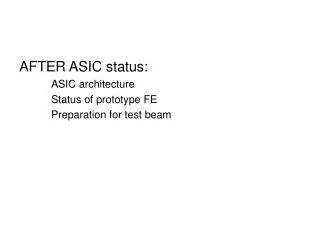
AFTER ASIC status: ASIC architecture Status of prototype FE Preparation for test beam. AFTER ASIC architecture. 76 channels/chip AMS CMOS 0.35 µm technology. Operation: analog ring buffer 511 cells trigger =>Delay => Stop programmable Depth T delay = T depth – T trigger latency.

E N D
AFTER ASIC status: ASIC architecture Status of prototype FE Preparation for test beam
AFTER ASIC architecture 76 channels/chip AMS CMOS 0.35µm technology • Operation: • analog ring buffer 511 cells • trigger =>Delay => Stop • programmable Depth • Tdelay = Tdepth – Ttriggerlatency
Signal shape Expected noise 500 e- Sampling clock 10-50 MHz ReadOut clock 20-40 MHz
P_AFTER module 1 P_AFTER module = 64 TPC channels FE module assembled in January
Current Readout scheme • ADC • Transition card • P_AFTER module • 4 P_AFTER/ADC
FE prototype status • Hardware (ADC, Transition card, P_AFTER) – READY • Firmware: • Access to configuration registers - READY • ReadOut control sequence – READY • Write Mode • Trigger • Delay for 1 - 511 clock cycles • Stop Write/Start Read • Read column wise for 1 – 511 columnes • Back to Write Mode • Read unsparsified Data – Being Developed • Zero suppression – next step
Preparation for test beam • ADC cards are in production – delivery in March • Complete Firmware • Readout of unsparsified DATA – by end of February • Zero suppression - June • Characterise AFTER chip performance - ? • Bug fix and production of 16 P_AFTER modules(1024 channels) – April
2 Readout arrangements 1 ADC card => 1024 TPC channels
AFTER chip availability • Saclay submitted production in January • 150 chips are booked • Price - ?