Pixel detector development for PANDA
Pixel detector development for PANDA. Rivetti INFN – Sezione di Torino. Major requirements. In PANDA the MVD is expected to contribute also to particle ID via dE/dx. Dynamic range: up to 2.5 MeV of deposited energy ( 700000 electrons).

Pixel detector development for PANDA
E N D
Presentation Transcript
Pixel detector development for PANDA • Rivetti • INFN – Sezione di Torino
Major requirements • In PANDA the MVD is expected to contribute also to particle ID via dE/dx. • Dynamic range: up to 2.5 MeV of deposited energy (700000 electrons). • Low momentum particles => low material budget. • About 120 modules and 1300 front-end chip will be needed. • Asymmetric hit rate distribution. • Global estimated rate: 1.025 GHz (50 Gbit/s) • Maximum hit rate per module: 34 MHz (1.7 Gbit/s) • Maximum hit rate per front-end chip: 5.8 MHz (290 Mbit/s) • Triggerless read-out • Front-end power < 200mW/chip. • Pixel size: 100 mm x 100 mm
Motivations for R&D • Custom front-end design motivated by the combination of: • Large dynamic range. • Pixel form factor. • Triggerless read-out. • Material budget • Eg. Tests done in Juelich show that the ATLAS chip used in “PANDA mode” is at the limit of rate required and would dissipate 330 mW/chip. • In this presentation: • Architecture of the front-end. • Results from a first prototype. • R&D work on epitaxial silicon sensors.
Front – end chip Basic features: • Chip size O(1 cm2 ). • Technology 0.13 mm CMOS. • Adequate radiation tolerance. • Buttable on three sides. • Capable of handling sensors of both polarities. • In each pixel: hit time and charge Pixel matrix Read – out logic
A first architecture • Column read-out ATLAS-like. • Chip read-out optimized for triggerless environment 3 tasks run simultaneously: • Hit detection in pixel and storage of time stamp • Readout of pixel data into the column FiFos • Readout of FiFos out of the FE
Event ordering • Three circuits in the chip ensures the proper time ordering of the hits in case of counter overflow. • The column controller, which generates a counter-overflow signal when the counter overflowsafter all “old” data in a column was read out. • The read-out controller. If a FIFO shows a CO event, its read-out is stopped till all the FIFO show a CO event. • The EoC event generator. The EoC is generated when all the FIFO show a CO event. The EoC mark is sent outside the chip and the CO flags are cleared.
Architecture simulations • Combined Monte-Carlo – VHDL simulations. • Simulation based on a sample of 120000 events on pbar on copper with a beam momentum of 4 GeV/c. • Full read-out cycle simulated on 68000 events. • 800 hit lost (1.18%) • Reasons for losses: • hit below threshold (set at 1200 electrons) • Pile-up on the ToT (0.5 %)
First prototype for PANDA • A first prototype was designed and tested. • Aim of the exercise: gain experience with the technology (very complex!) and explore the analogue performance. • 32 pixel cells with preamplifier with ToT and comparator. • Goal: keep the analogue power consumption below 12 mW pixel at 1.2V supply
Preamp schematic • Single stage preamplifier design to minimize power consumption • Feedback capacitor of 10fF nominal value • Calibration capacitor of 30 fF
Test board • The chip has been wired bonded to a small sensor provided by ITC – IRST (Trento).
Chip and sensor detail Fe chip IRST sensor
Preamp response to 0.5fC Noise@ 0pF: 98 e- rms
ToT linearity • Only the region up to 32fC can be explored through the injection capacitor • Preamplifier saturates at 12 fC.
A first spectrum ENC: 440 rms electrons Input capacitance about 1.5 pF
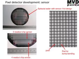
Epitaxial silicon sensor Lightly doped epitaxial layer r = 50 W cm • Several studies indicate that sensor build on epi wafer have good radiation tolerance. • Interest for PANDA: radiation tolerance adequate with standard p-type design. Highly doped Cz substrate: r = 0.01 – 0.02 W cm Wafers supplied by ITME and processed by ITC-IRST in Trento • Substrate properties: • Diameter: 100 ± 0.5 mm. • Doping type: n/Sb. • Thickness 525 ± 25 mm. • Resistivity: 0.01 – 0.02 W cm. • Epi layer properties: • Doping type n/P. • Thickness 50/75/100 mm. • Variation: <4%/8%/8% • Resistivity: 2500 – 5000 W cm.
Epi assemblies • Low cost R&D reusing existing electronics and sensor design: • Electronics: ALICE front-end chip provided by CERN • Sensor: masks developed by INFN-Ferrara for the P326 project. • Three types of epi assemblies: • 3 with 150 mm total thickness (100 mm epi) • 7 with 120 mm total thickness (75 mm epi) • 1 with 100 mm total thickness (50 mm epi) • Several wafers cracked during thinning (problem more severe on thicker wafer) • Problem probably due to stresses on the epi layer: work in progress to fix it • Good assemblies were however delivered and will be tested in May.
Summary • The R&D for a custom pixel detector for PANDA has been started. • The architecture of front-end chip is under development. • Design is not yet frozen, many changes still possible! • A first analogue prototype has been designed and tested in 0.13mm. • Good performance obtained for noise, dynamic range, linearity. • The analogue part has been operated with 12 mW/pixel. • The results are in reasonable agreement with simulations. • The technology is significantly more complex than the 0.25 mm, but it offers several interesting options (triple-well NMOS, analogue components, thicker oxide devices for I/Os, etc..)
Credits • Thanks to the many people working on the project in several ways… D. Calvo, P. Deremigis, G. Mazza, S. Martoiu, M. Mignone, R. Wheadon, K. Brinkmann, F. Huegging, T. Stocksmann, R. Jäkel, M. Mertens, J . Ritman… • Thanks to the organizers for the invitation!
Some design considerations in 0.13 mm • Mobility very different between PMOS and NMOS devices (kN/kP~6). • The use of NMOS transistor to control small currents becomes problematic (problem much more severe than in 0.25 mm). • NMOS input with triple-well and splitted PMOS current sources is probably the best compromise.
Issues related to ToT technique • The preamplifier saturates at 12 fC, but the ToT preserves good “linearity” at least up to 40 fC. • Caveat: in the saturated region the open-loop gain of the input stage drops down, making the system more prone to cross-talk. Cin=Cf(1+A0)>>Cd Cf=10fF, Cd=200fF Cin=Cd for A0=20
Adjacent Coupled Detectors Pixel Matrix Particle hit Jin1 0 CC Jin2= 0 hit event Jin2 Jin1 CD CD no hit event Equivalent Circuit hit event Cf Cf Injected charge Vo2 Vo1 - + - + detector01 CSA01 no hit event CC detector02 CSA02 Mastering cross talk • The cross-talk with a saturated preamplifier can go up to 20%. • Possible remedies: • 1. Guard-ring connected to ground • 2. Two stage preamplifier, with first stage working always in linearity


