Download
1 / 40
400 likes | 584 Vues
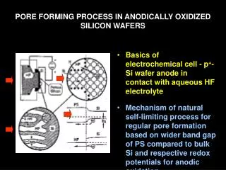
PORE FORMING PROCESS IN ANODICALLY OXIDIZED SILICON WAFERS. Basics of electrochemical cell - p + -Si wafer anode in contact with aqueous HF electrolyte

E N D
PORE FORMING PROCESS IN ANODICALLY OXIDIZED SILICON WAFERS • Basics of electrochemical cell - p+-Si wafer anode in contact with aqueous HF electrolyte • Mechanism of natural self-limiting process for regular pore formation based on wider band gap of PS compared to bulk Si and respective redox potentials for anodic oxidation
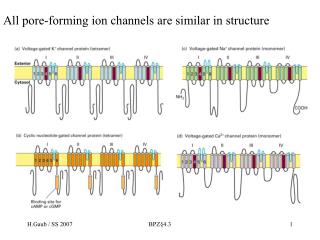
KEY ISSUES: ORIGIN OF PHOTO- AND ELECTROLUMINESCENE OF POROUS SILICON • Origin of luminescence key point- as bulk Si is indirect band gap semiconductor with very weak light emission • Models for light emission include quantum-spatial confinement, siloxenes, and SiOH • Luminsecent nc-Si structure requires SiO, SiH surface bonds - caps dangling bonds -removes killer traps in band gap • Size dependence of k, m selection rules, scaling laws determine light emission properties • Mechanical, photochemical, chemical stability are key factors for devices • Efficient e-h charge-injection required for practical LED
*(SiH) CB CB capping Si cluster dangling bond with H, F, O forms bonding-antibonding -orbitals, moves killer trap states out of the gap facilitates radiative relaxation VB VB (SiH) Sin HxSin MAKING NANOCRYSTALLINE SILICON LUMINESCENT: CAPPING
THERMAL OXIDATION FORMATION OF METAL OXIDE AND NITRIDE THIN FILMS • Anodic layers, metal exposed to a glow discharge • Ti + O2 TiO2 thickness 3-4 nm • Similar method applicable to other metals, Al, V, W, Zr • Not restricted to oxides, nitrides too, exceptionally hard, high temperature protective coating • Ti + NH3 TiN • Al + NH3 AlN
CHEMICAL VAPOUR DEPOSITION • Pyrolysis, photolysis, chemical reaction, discharges, RF, microwave facilitated deposition processes • Epitaxial films, correct matching to substrate lattice • CH4 + H2 (RadioF, MicroW) C, diamond films • Et4Si (thermal, air) SiO2 • SiCl4 or SiH4 (thermal T, H2) a-H:Si or nc-H:Si • SiH4 + PH3 (RF) n-Si
CHEMICAL VAPOUR DEPOSITION • Si2H6 + B2H6 (RF) p-Si • SiH3SiH2SiH2PH2 (RF) n-Si • Me3Ga (laser photolysis, heating) Ga • Me3Ga + AsH3 + H2 GaAs + CH4 • Si (laser evaporation, supersonic jet) Sin+ (size selected cluster deposition) Si
H H H H H H H H H H H H H H H H H H H H H H H H H H H H H H H H H H H Amorphous hydrogenated silicon a-H:Si, easy to form thin film by CVD Hydrogen capping of dangling surface sp3 bonds Reduces surface electron killer traps Enhances electrical conductivity compared to a-Si but less than bulk Si Poly-domain texture Useful for solar cell large area devices
METAL ORGANIC CHEMICAL VAPOR DEPOSITION, MOCVD • Invented by Mansevit in 1968 • Recognized high volatility of metal organic compounds as sources for semiconductor thin film preparations • Enabling chemistry for electronic and optical quantum devices • Quantum wells and superlattices • Occurs for 5-500 angstrom layers • Known as artificial superlattices
Schematic energy band diagram of a quantum well structure showing confined electron and hole states produced by large Eg GaAlAs layers sandwiching small Eg GaAs depicting quantization effects and some possible optical transitions CB edge GaAlAs CB/VB edges GaAs L VB edge GaAlAs En = n2p2h2/2m*L2
METAL ORGANIC CHEMICAL VAPOR DEPOSITION, MOCVD • Quantum confined electrons and holes when thickness of quantum well L is comparable to the wavelength of an electron or hole at the Fermi level of the material, band diagram shows confined particle states and quantization effects for electrical and optical properties • Discrete electronic energy states rather than continuous bands, given by solution to the simple particle in a box equation, assuming infinite barriers for the wells, m* is the effective mass of electrons and holes • En = n2p2h2/2m*L2 • Tunable thickness, tailorable composition materials, do it yourself quantum mechanics materials for the semiconductor industry
METAL ORGANIC CHEMICAL VAPOR DEPOSITION, MOCVD • Quantum well structure synthesized by depositing a controlled thickness superlattice of a narrow band gap GaAs layer sandwiched by two wide band gap GaxAl1-xAs layers using MOCVD • Ga(Al)Me3 + AsH3 (H2, T) Ga(Al)As + CH4 • Known as artificial superlattices, designer periodicity of layers, quantum confined lattices, thin layers, epitaxially grown • Example: GaxAl1-xAs|GaAs|GaxAl1-xAs
MOCVD • Example: GaxAl1-xAs|GaAs|GaxAl1-xAs • n- and p-doping achievable by having excess As or Ga respectively in a GaAs layer • Composition and carrier concentration controls refractive index and electrical conductivity, thus TIR achieved in a semiconducting superlattice • Enables quantum and photon confinement for electronic and optoelectronic and optical devices, multiple quantum well laser, quantum cascade laser, distributed feedback laser, resonant tunneling transistor, high mobility ballistic transistor, laser diode
BAND GAP ENGINEERING OF SEMICONDUCTORS • The MOCVD, LPE, CVD, CVT, MBE are all deposition techniques that provide angstrom precise control of film thickness • Together with composition control one has a beautiful synthetic method for fine tuning the electronic band gap and hence most of the important properties of a semiconductor quantized film • The key thing is to achieve epitaxial lattice matching of the film with the underlying substrate • This avoids things like lattice strain at the interface, elastic deformation, misfit dislocations, defects • All of these problems serve to increase carrier scattering and quenching of e-h recombination luminescence (killer traps), thereby reducing the efficacy of the material for advanced device applications
MOCVD PRECURSORS, SINGLE SOURCE MATERIALS • Me3Ga, Me3Al, Et3In • NH3, PH3, AsH3 • H2S, H2Se • Me2Te, Me2Hg, Me2Zn, Me4Pb, Et2Cd • Example for IR detectors: • Me2Cd + Me2Hg + Me2Te (H2, 500oC) CdxHg1-xTe • All pretty toxic materials
MOCVD PRECURSORS, SINGLE SOURCE MATERIALS • Specially designed MOCVD reactors, hot and cold wall designs, controlled flow of precursors using mass flow meters directing them to heated substrate single crystal, induction heater, silicon carbide coated graphite susceptor for mounting substrate • Chemistry of this type creates a problem for semiconductor manufacturers in terms of safe disposal of toxic waste • Most reactions occur in range 400-1300oC, complications of diffusion at interfaces, disruption of atomically flat epitaxial surfaces/interfaces occurs during deposition • Photolytic processes (photoepitaxy) help to bring the deposition temperatures to more reasonable temperatures
MOCVD surface chemistry of precursors, nucleation and growth of product film Me Me Me CH4 Ga Me Me Me Me Me H H H Ga Al As Me H As Al As Al As Al As Al As Al As Al As Al As Al As Al As Precursor adsorption on single crystal oriented substrate - lattice matching epitaxy criteria - surface physisorption - chemisorption - surface diffusion - dissociative chemisorption - reaction - desorption Different models for film nucleation and growth - depends whether surface diffusion involved - fixed vs mobile crystal nuclei
Schematic of cold wall MOCVD system Single crystal substrate on inductively heated or resistively heated susceptor MOCVD deposited film H2/AsH3/PH3 Water cooling H2/InMe3/GaMe3 Thermocouple H2/PEt3 H2/n-dope H2S/p-dope ZnMe2 Waste gases
REQUIREMENTS OF MOCVD PRECURSORS • RT stable • No polymerization, decomposition • Easy handling • Simple storage • Not too reactive • Vaporization without decomposition
REQUIREMENTS OF MOCVD PRECURSORS • Vaporization without decomposition • Modest < 100oC temperatures • Low rate of homogeneous pyrolysis, gas phase, wrt heterogeneous decomposition • HOMO : HETERO rates ~ 1 : 1000 • Heterogeneous reaction on substrate • Greater than on other hot surfaces in reactor
REQUIREMENTS OF MOCVD PRECURSORS • Not on supports, vessel • Ready chemisorption of precursor on substrate • Detailed surface and gas phase studies of structure of adsorbed species, reactive intermediates, kineticss, vital for quantifying film nucleation and growth processes • Electronic and optical films synthesized in this way • Semiconductors, metals, silicides, nitrides, oxides, mixed oxides (e.g., high Tc superconductors)
CRITICAL PARAMETERS IN MATERIALS PREPARATION FOR SYNTHESIS OF THIN FILMS • Composition control - precise command over stoichiometry and adventitious carbonaceous deposits • Variety of materials to be deposited • Good film uniformity • Large areas to be covered, > 100 cm2 • Precise reproducibility
CRITICAL PARAMETERS IN MATERIALS PREPARATION FOR SYNTHESIS OF THIN FILMS • Growth rate, thickness control • 2-2000 nm layer thicknesses • Precise control of film thickness • Accurate control of deposition, film growth rate
CRITICAL PARAMETERS IN MATERIALS PREPARATION FOR SYNTHESIS OF THIN FILMS • Crystal quality, epitaxy • High degree of film perfection • Defects degrade device performance • Reduces useable wafer yields
CRITICAL PARAMETERS IN MATERIALS PREPARATION FOR SYNTHESIS OF THIN FILMS • Purity of precursors • Usually less than 10-9 impurity levels • Stringent demands on starting material purity • Challenge for chemistry, purifying and analyzing at the ppb level • Demands exceptionally clean growth system otherwise defeats the object of controlled doping of films for device applications
CRITICAL PARAMETERS IN MATERIALS PREPARATION FOR SYNTHESIS OF THIN FILMS • Interface widths • Abrupt changes of composition, dopant concentration required, vital for quantum confined structures • 30-40 sequential layers often needed • Alternating composition and graded composition films • 0.5-50 nm thicknesses required with atomic level precision • All of the above has been more-or-less perfected in the electronics and optics industries
TECHNIQUES USED TO GROW SEMICONDUCTOR FILMS AND MULTILAYERED FILMS • MOCVD • Liquid phase epitaxy • Chemical vapor transport • Molecular beam epitaxy • Laser ablation • Used for band gap engineering of semiconductor materials that function at 1.5 microns in near IR - integrating with glass fiber optics and waveguides
BAND GAP ENGINEERING • Designer semiconductors • Zinc blende lattice • Lattice constant • Composition • Doping • Thickness • Multilayers • Epitaxial lattice matching • Control of band gap and refractive index • Operating wavelengths for optical telecommunication systems labeled in purple
TAILORED BAND GAPS - DESIGNER MOCVD GRADED COMPOSITION POTENTIAL WELLS AlxGa1-xAs graded composition-gap superlattice CB AlAs wide gap e CB GaAs narrow gap Tunable h VB GaAs narrow gap h VB AlAs wide gap Designer quantum well architecture - band gap engineering - graded potential can be used to enhance electron mobility in HEMTs or build a quantum cascade laser
Federico Capasso co-inventor of the quantum cascade laser imagined small things when he used size and dimensionality of materials to tailor their properties for electronic and optical devices
QUANTUM CASCADE LASER; A NICE EXAMPLE OF BAND GAP ENGINEERING BY MOCVD The white bands in the TEM are QWs made of GaInAs, which are sandwiched between barrier layers of AlInAs ranging in thickness from atomic to 12 atomic layers . All the wells are part of a quantum cascade laser. When a voltage is applied to the device, electrons move down the potential barrier from narrow to wide band QWs and emit a photon between the two thickest QWs. Then the electron moves on to the next stage to the right where the process repeats.
Cathode material to be sputtered single or multi-target + Power supply - Inert gas inlet Ar M M M Substrate (anode) Vacuum
PHYSICAL METHODS FOR MAKING THIN FILMS • CATHODE SPUTTERING • Bell jar equipment, 10-1 to 10-2 torr of Ar, Kr, Xe • Glow discharge created, positively charged rare gas ions, accelerated in a high voltage to cathode target, high energy ions collide with cathode • Sputter material from cathode, deposits on substrate opposite cathode to form thin film • Multi-target sputtering also possible, creates composite or multi-layer films
PHYSICAL METHODS FOR MAKING THIN FILMS • THERMAL VACUUM EVAPORATION • High vac bell jar > 10-6 torr, heating: e-beam, resistive, laser • Gaseous material deposits on substrate, film nucleates and grows • Containers must be chemically inert, W, Ta, Nb, Pt, BN, Al2O3, ZrO2, Graphite • Substrates include insulators, metals, glass, alkali halides, silicon, sources include metals, alloys, semiconductors, insulators, inorganic salts
CONTROL OVER THIN FILM GROWTH AT THE ATOMIC SCALE: MOLECULAR BEAM EPITAXY
MOLECULAR BEAM EPITAXY Structure of thin film Vapor phase species control Ar+ ion gun for cleaning substrate surface or depth profiling Surface analysis Elemental sources in shuttered Knudsen cells
MOLECULAR BEAM EPITAXY - MBE • Million dollar thin film machine, ideal for preparing high quality artificial semiconductor quantum superlattices, ferroelectrics, superconductors • Ultrahigh vacuum system >10-12 torr, what's in the chamber? • Elemental or compound sources in shutter controlled Knudsen effusion cells, Ar+ ion gun for cleaning substrate, surface or depth profiling sample using Auger analyzer, high energy electron diffraction for surface structure analysis, mass spectrometer for control and detection of vapor species, e-gun for heating the substrate
Bottom graphite, middle substrate, top HgTe film H2 gas window Hg pool H2/Et2Te Exhaust gases UV illumination PHOTOEPITAXYMaking atomically perfect thin films under milder and more controlled conditionsEt2Te + Hg + H2 (h, 200oC) HgTe + 2C2H6