Download
1 / 12
120 likes | 252 Vues
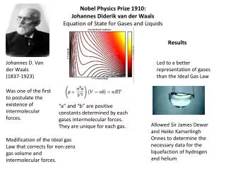
Using Atomic Diffraction to Measure the van der Waals Coefficient for Na and Silicon Nitride J. D. Perreault 1,2 , A. D. Cronin 2 , H. Uys 2 1 Optical Sciences Center, University of Arizona, Tucson AZ, 85721 USA 2 Physics Department, University of Arizona, Tucson AZ, 85721 USA. Abstract.

E N D
Using Atomic Diffraction to Measure the van der Waals Coefficient for Na and Silicon Nitride J. D. Perreault1,2, A. D. Cronin2, H. Uys2 1Optical Sciences Center, University of Arizona, Tucson AZ, 85721 USA 2Physics Department, University of Arizona, Tucson AZ, 85721 USA
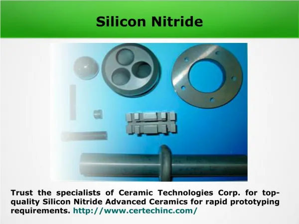
Abstract In atom optics a mechanical structure is commonly regarded as an amplitude mask for atom waves. However, atomic diffraction patterns indicate that mechanical structures also operate as phase masks. In this study a well collimated beam of Na atoms is used to illuminate a silicon nitride grating with a period of 100 nm. During passage through the grating slots atoms acquire a phase shift due to the van der Waals (vdW) interaction with the grating walls. This phase shift depends both on atom position and velocity. As a result the relative intensities of the matter-wave diffraction peaks deviate from optical theory and depend on the de Broglie wavelength of the atoms. The vdW coefficient C3 is determined by fitting a modified Fraunhoffer optical theory to the experimental data.
x x z z Na 100 nm period diffraction grating 60 μm diameter hot wire detector 10 μm collimating slits .5 μm skimmer supersonic source Experiment Geometry • A supersonic Na atom beam is collimated and used to illuminate a diffraction grating • A hot wire detector is scanned to measure the atom intensity as a function of x
van der Waals Diffraction Theory • The far-field diffraction pattern for a perfect grating is given by • The diffraction envelope amplitude An is just the scaled Fourier transform of the single slit transmission function T(x) • Notice that T(x) is complex when the van der Waals interaction is incorporated and the phase following the WKB approximation to leading order in V(x) is
Definitions ldB: de Broglie wavelength v: velocity sv: velocity distribution d: grating period w: grating slit width t: grating thickness I(x): atom intensity An: diffraction envelope amplitude |An|2: number of atoms in order n T(x): single slit transmission function V(x): vdW potential f(x): phase due to vdW interaction x: grating coordinate fx: Fourier conjugate variable to x x: detector coordinate z: grating-detector separation L(x): line shape function n: diffraction order
optical phase front negative lens Intuitive Picture • As a consequence of the fact that matter propagates like a wave there exists a suggestive analogy • The van der Waals interaction makes each slot act as a lens, adding curvature to the de Broglie wave fronts and thus modifying the far-field diffraction pattern
grating rotation experiment: SEM image: w = 68.44 ± .01 nm Measuring the Grating Parameters • A grating rotation experiment along with an SEM image are used to independently determine the grating parameters w and t and g.
Determining |An|2 • Free parameters: |An|2, v, σv • The background noise and lineshape function L(x) are determined from an independent experiment
Preliminary Results: Best Fit C3 C3 = 5.95 ± .45 meVnm3 (statistical error only) C3 = 3.13 ± .04 meVnm3 (statistical error only) • The relative number of atoms in each diffraction order was fit with only one free parameter: C3 • Notice how optical theory (i.e. C3=0) fails to describe the diffraction envelope correctly for atoms.
Using Zeroeth Order Diffraction to Measure C3 • Using the previously mentioned theory one can see that the zeroth order intensity and phase depend on the strength of the van der Waals interaction • The phase shift could be measured in an interferometer to determine C3 • The ratio of the zeroeth order to the raw beam intensity could be used to measure C3
Conclusions and Future Work • A preliminary determination of the van der Waals coefficient C3 for Na on silicon nitride has been presented here for two different atom beam velocities based on the method of Grisenti et. al • Using the phase and intensity dependence of the central diffraction order on C3 we are pursuing novel methods for the measurement of the van der Waals coefficient • The van der Waals phase could be “tuned” by rotating the grating about its k-vector, effectively changing the value of t by some known amount
References “Determination of Atom-Surface van der Waals Potentials from Transmission-Grating Diffraction Intensities” R. E. Grisenti, W. Schollkopf, and J. P. Toennies. Phys. Rev. Lett. 83 1755 (1999) “He-atom diffraction from nanostructure transmission gratings: The role of imperfections” R. E. Grisenti, W. Schollkopf, J. P. Toennies, J. R. Manson, T. A. Savas and H. I. Smith. Phys. Rev A. 61 033608 (2000) “Large-area achromatic interferometric lithography for 100nm period gratings and grids” T. A. Savas, M. L. Schattenburg, J. M. Carter and H. I. Smith. Journal of Vacuum Science and Technology B 14 4167-4170 (1996)