Advanced FADC Receiver & Driver Design with Flexible DSP Algorithm Implementation
Explore an innovative design for a 10-channel FADC receiver and driver system featuring advanced DSP capabilities. This setup integrates the CPLD, CPU, and FPGA for efficient data handling and processing, including zero dead time and customizable function selection. Key advantages include the ability to install multiple algorithms in the DSP, facilitating enhanced performance. The architecture allows modular division of blocks without operational conflicts, supporting dual-port RAM and ensuring seamless communication with the VME bus. Optimize your data acquisition system today!

Advanced FADC Receiver & Driver Design with Flexible DSP Algorithm Implementation
E N D
Presentation Transcript
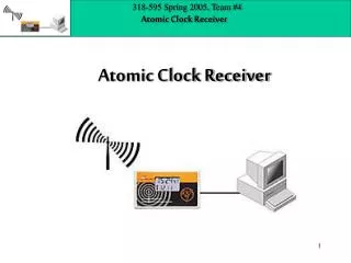
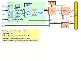
x8 Download EEPROM FADC Block Download EEPROM Receiver & Driver 10 FADC CH 1 CPLD DSP CPU Read Write VA[8..15] VA[8..15] 10 Receiver & Driver Pre-Processing FPGA FADC Dual-port FIFO DSP Read DSP Read CH 2 VD[0..31] VA[8..15] VD[0..31] CS VME Bus 10 Receiver & Driver Flag 4 FADC CH 3 VD[0..31] Receiver & Driver 10 FADC CH 4 Write CPU Read VD[0..31] Clock Dual-port RAM Trigger JTAG Reset This design has some advantages as follows: (1). Zero Dead time. (2). More algorithm can be installed into the DSP. (3). User can select the functions which he wants. (4). Divide each block into individual modulw without conflict.
x8 Download EEPROM FADC Block Download EEPROM Receiver & Driver 10 FADC CH 1 CPLD DSP CPU Read Write VA[8..15] 10 Receiver & Driver Pre-Processing FPGA DSP Read DSP Read FADC CH 2 VA[8..15] VD[0..31] CS VME Bus 10 Receiver & Driver FADC CH 3 VD[0..31] Receiver & Driver 10 FADC CH 4 Write CPU Read VD[0..31] Clock Dual-port RAM Trigger JTAG Reset This design has some advantages as follows: (1). Zero Dead time. (2). More algorithm can be installed into the DSP. (3). User can select the functions which he wants. (4). Divide each block into individual modulw without conflict.