Download
1 / 36
360 likes | 398 Vues
Learn about the Serial Peripheral Interface (SPI) technology, including data transmission, clock synchronization, and device selection. Configure and operate SPI on the 68HC11 using AS11. Explore SPI registers and transfer formats. Utilize SPI for parallel I/O and efficient data transfer.

E N D
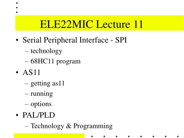
ELE22MIC Lecture 11 • Serial Peripheral Interface - SPI • technology • 68HC11 program • AS11 • getting as11 • running • options • PAL/PLD • Technology & Programming
Serial Peripheral Interface (SPI 2) During an SPI transfer, data is simultaneously transmitted (shifted out serially) and received (shifted in serially). A serial clock line synchronises shifting and sampling of the information on the two serial data lines. A slave select line allows individual selection of a slave SPI device; slave devices that are not selected do not interfere with SPI bus activities. On a master SPI device, the slave select line can optionally be used to indicate a multiple-master bus contention.
Serial Peripheral Interface (SPI 3) Simplest Form: The SPI can be used to add an extra 8 bit output port using an 8-bit shifter and latches. Master Out Slave In MOSI (Serial Data) -> Pin14 (MS bit sent first) Clock ->Pin 11 SS# = Pin 12 = Low during transmission Reset# = Pin 10 = 5V OE# = Pin 13 = 0V
Serial Peripheral Interface (SPI 4) Configuring SPI - From Technical Data 11A8TD.pdf, P29.
Serial Peripheral Interface (SPI 5) Four major registers influence SPI usage: 1. SPI Control Register (SPCR at $1028), 2. SPI Status Register (SPSR at $1029), and 3. SPI Data Register (SPDR at $102A) 4. Data Direction Register for port D (DDRD at $1009) These are software-accessible registers used to configure and operate the SPI system. Detailed logic diagrams of the port D pins can be found in 68HC11 Reference Manual SECTION 7 PARALLEL INPUT/OUTPUT (ELE22MIC cdrom:\MotorolaDatasheets\11rm.pdf)
Serial Peripheral Interface (SPI 6) Transfer Format: Data Out is Clocked with Rising SCK , when CPOL = 0 (CPOL = BIT3 of SPI Control Register (SPCR)
Serial Peripheral Interface (SPI 7) SCK Bit Rate Select when 68HC11 is selected as Master is defined by SPR1 & SPR0 from SPCR
Serial Peripheral Interface (SPI 8) Data Direction Register D (DDRD) - This register, which may be read or written at any time, is used to control the primary direction of port D pins. Bits 5, 4, 3, and 2 of port D are used by the SPI system when the SPI Enable (SPE) control bit is one. The Serial Communications Interface (SCI) system uses the other two bits of port D when the SCI receiver and transmitter are enabled. This description of DDRD is only intended to cover material related to the SPI system.
Serial Peripheral Interface (SPI 9) Data Direction Register D (DDRD) - DDRD5 — Data Direction Control for Port D Bit 5 (SS) When the SPI system is enabled as a master (SPE = 1; MSTR = 1), the function of the PD5/SS pin depends on the value in DDRD5. When the SPI system is enabled as a slave (SPE = 1; MSTR = 0), the PD5/SS pin is the slave select input, regardless of the value of DDRD5. See also Section 8.5.1 SPI Mode-Fault Error - Upon detection of mode error, all SPI pins are set to inputs.
Serial Peripheral Interface (SPI 10) Data Direction Register D (DDRD) - DDRD4 — Data Direction Control for Port D Bit 4 (SCK) When the SPI system is enabled as a master, the DDRD4 bit must be set to one to enable the SCK as an output. When the SPI system is enabled as a slave, the PD4/SCK pin acts as the SPI serial clock input, regardless of the state of DDRD4.
Serial Peripheral Interface (SPI 11) SPI Master-Slave Interconnection Notes: Master generates SPI clock, SS - Slave Select - is hard-wired low for slave Image from 68HC11A8 Technical Data (11atd.pdf)
SPI Write Assembly Code (SPI CODE 1) ACCESS_SPI: LDAA #50 ; 0101 00002 ; BIT7 = 0 = SPIE = Interrupts Disabled ; BIT6 = 1 = SPE = SPI System Enabled ; BIT5 = 0 = DWOM = outputs are push-pull ; 1 = DWOM = Port D Wired OR Mode ; BIT4 = 1 = MSTR = SPI MaSTeR Mode Select ; BIT3 = 0 = CPOL = Clock Polarity Select ; BIT2 = 0 = CPHA = Clock Phase Select ; BIT1/0= 0,0 = Bit Rate Select = E Clk / 2 STAA 1028 ; SPI Control Register (SPCR) * If CPHA = 0, SS# must be toggled every 8 bits. * If CPHA = 1, SS# may remain active-low between 8 bit transfers. * This is useful for sending multi-bytes transfers
SPI Write Assembly Code (SPI CODE 2) * Configure the port D Pins used for SPI LDAA #38 ; 0011 10002 ; BIT7 & 6 = 0, 0 = Unused Bits - Don’t exist on port D ; BIT5 = 1 = Configure for output SS# ; BIT4 = 1 = Configure for output SCLK ; BIT3 = 1 = Configure for Output MOSI ; BIT2 = 0 = Configure for Input MISO ; BIT1 = 0 = SCI Transmit Data = TxD ; BIT0 = 0 = SCI Receive Data = RxD STAA 1009 ; DDRD - Data Direction Register for Port D
SPI Write Assembly Code (SPI CODE 3) LDAA #55 ; 0101 01012 - Data to send to SPI Slave STAA 102A ; SPI Data Register = SPDR PollAgain: LDAB 1029 ; Read SPI Status Register = SPSR ; Acc B = Status of SPI ; BIT7 = SPIF = 1 => SPI Transfer is Complete ; BIT6 = 1 => WCOL = SPI Write Collision ; Write to data register while transfer is taking place ; BIT4 = MODF = SPI Mode Fault, Normally 0 ; Set to 1 = Multi Master Conflict -> Disables SPI ; Bits 5, 3-0 always return 0. BITB #80 ; AND SPIF bit - Transfer Complete? BEQ PollAgain ; If still 0, keep waiting. ; could use: ; PollAgain: ; …. ; BRCLR 1029, PollAgain
SPI Write Assembly Code (SPI CODE 4) BCLR $1008 20 ; 1008 = Port D = Strobe Bit 5 Low = SS BSET $1008 20 ; 1008 = Port D = Strobe Bit 5 High = SS * We have sent byte via SPI, now return to the calling routine RTS ; Return from Subroutine
Instruction Cycle times • Different instructions take varying lengths of time. • Sometimes this is important to know exactly how long a section of will take to execute. • This can be calculated by looking up the number of cycles each instruction takes, and adding them together. • Another way is to get the assembler to list them for you.
Example Assembler org 2000 ; Uses: = N, CCR NSomethings: ; RepeatAgain: ; repeat { JSR DoSomething ; { DoSomething () // do it A times DEC N ; N--; ; } BNE RepeatAgain ; until (N == 0) ExitLoop: RTS org 2100 N RMB 1 ; RMB = Reserve Memory Byte
Getting AS11 To get AS11 visit the URL: http://thor.ee.latrobe.edu.au/~paulm/ele22mic/index.html at the bottom of the page, right click on the link AS11 Assembler and select “Save Target As” to a local directory d:\as11 for example. Also available from your ELE22MIC CDROM / textbook CDROM.
AS11 Assembler Invocation To invoke the cross-assembler AS11 in a dosbox enter: AS11 file1 (file2...) -option1 -option2 Options: l enable output listing. nol disable output listing (default). cre generate cross reference table. s generate a symbol table. c enable cycle count. noc disable cycle count.
PLD Technology (1) Equations can be written to describe the required logic arrangement. Next the equations can be compiled to produce a JEDEC file, and then loaded into the PAL using a device programmer. In the event that an error in logic was made, re-programming the PLD can correct the design error without modifying the Printed Circuit Board.
PLD Technology (4) The 22V10 Programmable Logic Device (PLDs) is a popular choice to generate necessary glue logic for microprocessor designs. By using one programmable device designers can save on many other Small Scale Integration devices, and also save power. PLDs can be based on EPROM, EEPROM or FLASH technology.
Configuring a PAL/PLD (1) • Programmable Array Logic (PALs) or Programmable Logic Devices (PLDs) can be configured by setting / resetting “fuse” links. • There are many logic device families and programming languages for example: • For PALs: PALASM, CUPL, or Schematic Entry • For FPGAs: Varilog, VHDL, ABLE, Schematic • Protel’s Advanced PLD allows you to design using logic in a schematic, or the CUPL/VHDL language, and then compile to a JEDEC, ready to program into a PLD
Example CUPL Program (1) Name AddressDecode14; Partno MV12C; Revision 03; Date 19 June, 2001; Designer Paul Main; Company Systems Engineering Arts Pty Ltd; Assembly MV12C03 -> PC104 Modem Control lines; Location U1; Device G20V8; /************************************************************************/ /* Commercial Prototype */ /* This device decodes the PC104 address bus and generates enable */ /* signals for the serial port, the tone detector port & Control Reg. */ /* The base address is set at 2E0..2EF. */ /* CardSelect is determined by comparing 8 bits, A10-A3 of the PC104 bus*/ /* with 2Ex. (8 addresses will fold from 2E0..2E7 to 2E8..2EF) */ /* When the address matches and address enable (AEN) is low then */ /* Card Select signal is generated. */ /* Address bits PA2..PA0 are used to select which port: */ /* DetectorRead = CardSelect & (PA2 = 1 & PA1 = 1 & PA0 = 1) */ /* ModemSelect = CardSelect & (PA2 = 1 | PA1 = 1 | PA0 = 1) */ /* DetectIOR /* */ /************************************************************************/ /* Allowable Target Device Types: PALCE20V8 */ /************************************************************************/
Example CUPL Program (2) /** Inputs **/ pin 1 = !aen ; /* PC's address enable strobe */ pin [2..11,13] = [sa10..0] ; /* system address pins sa0 - sa10 */ pin 17 = !IOW ; /* IO Write strobe */ pin 18 = !IOR ; /* IO Read Strobe */ /** Outputs **/ pin 19 = !ModemRead ; /* modem read enable */ pin 20 = !ModemSelect ; /* modem select for read or write */ pin 21 = DetWrite ; /* 74HC374 is Rising edge triggered */ pin 22 = !DetRead ; /* tone detector port */ pin 16 = CardAddr ; /* The card is selected - modem or detectors */ /** Declarations and Intermediate Variable Definitions **/ field CardAddress = [sa10..0] ; /** Logic Equations **/ CardAddr = CardAddress:[2E0..2Ef] ; /* select modem for io addr 2e8 to 2ef */ ModemSelect= CardAddr & sa3 & aen ; /* Modem Buffer read/write control */ ModemRead = ModemSelect & IOR ; /* Modem Buffer read/write control */ DetWrite = CardAddr & !sa3 & aen & IOW ; /* Detector latch is selected on write to i/o address 2e0.. */ DetRead = CardAddr & !sa3 & aen & IOR ; /* Detector buffer is selected on read from i/o address 2e0.. */
Example JEDEC (1) ADVANCED PLD 4.0 Serial# MW-67999999 Device g20v8ma Library DLIB-h-36-3 Created Mon Aug 25 19:09:47 2003 Name AddressDecode14 Partno MV12C Revision 03 Date 19 June, 2001 Designer Paul Main Company Systems Engineering Arts Pty Ltd Assembly MV12C03 -> PC104 Modem Control lines Location U1 *QP24 *QF2706 *G0 *F0 *L00000 11111111111111111111111111111111 *L00032 11111111111011111111111111111110
Example JEDEC (1) *L00064 11111001111111110000000000000000 *L00320 11111111111111111111111111111111 *L00352 11111111111011111111111111111111 *L00384 11101001111111110000000000000000 *L00640 11111111111111111111111111111111 *L00672 11111111111011111111111111111111 *L00704 11110101111111110000000000000000 *L00960 11111111111111111111111111111111 *L00992 11111111111111111111111011111110 *L01024 11111111111111110000000000000000 *L01920 11111111111111111111111111111111 *L01952 11111111101101111011011101110111 *L01984 10111111111111110000000000000000 *L02560 01000010010011010101011000110001 *L02592 00110010010000110000000000000000 *L02624 00000000111111111111111111111111 *L02656 11111111111111111111111111111111 *L02688 111111111111111111 *C3AD9 *02C5
PLD in Circuit The chip select lines are now decoded for the four output terms: Pin 22= DetEnableRd#, Pin 21 = DetEnableWr#, Pin 20 = ModemSelect#, Pin 19 = ModemRead# Pin 16 = TP3 = CardAddr Top: 20V8 PAL Middle: Logic Container Bottom: PC104 bus interface
Acknowledgements • I used Altium Protel 98 and Protel DXP to create these schematic diagrams • Motorola 68HC11 Reference Manual (11rm.pdf ) • Motorola 68HC11A8 Technical Data (11a8td.pdf )