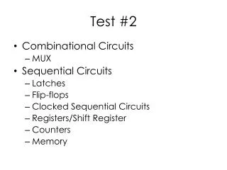
Test #2
Test #2. Combinational Circuits MUX Sequential Circuits Latches Flip-flops Clocked Sequential Circuits Registers/Shift Register Counters Memory. Multiplexer. 2-to-1 mux 4-to-1 mux. 2-to-1 mux. A 2-input mux is controlled by a single control line s . If s=0, y=a and y=b if s=1.

Test #2
E N D
Presentation Transcript
Test #2 • Combinational Circuits • MUX • Sequential Circuits • Latches • Flip-flops • Clocked Sequential Circuits • Registers/Shift Register • Counters • Memory
Multiplexer • 2-to-1 mux • 4-to-1 mux
2-to-1 mux • A 2-input mux is controlled by a single control line s. • If s=0, y=a and y=b if s=1.
4-to-1 Mux (Creating a 4 x 1 MUX from 2 x 1 MUX)
Latches • Latches are level sensitive. • Latches propagate values from input to output continuously. • S sets Q =1; R sets Q=0 • Active low inputs are enabled by 0s. • Active high inputs are enabled by 1s.
SR Latch with NOR Gates Active High inputs tPDSQ=2 NOR gate delays. tPDRQ_=1 NOR gate delay SR are trigger pulses which can return to zero once Q is set. Forbidden State
Typical Mode of Operation R must go back to 0 in order to avoid S=R=1. Q and Q’ do not change states when R goes back to 0. S must go back to 0 in order to avoid S=R=1. Q and Q’ do not change states when S goes back to 0. Both inputs of the latch remain at 0 unless the state has to be changed. When both S and R are equal to 0, the latch can be in either the set or the reset, depending on which input was most recently a 1.
SR Latch with NAND Gates S must go back to 1 in order to avoid S=R=0. Q and Q’ do not change states when S goes back to 1. R must go back to 1 in order to avoid S=R=0. Q and Q’ do not change states when R goes back to 1. Both inputs of the latch remain at 1 unless the state has to be changed. When both S and R are equal to 1, the latch can be in either the set or the reset, depending on which input was most recently a 1.
Comparison (activated with a 1) (activated with a 0)
SR Latch with NAND Gates Active low inputs
SR latch with Control Line (En=0) 1 0 1 1. En=0, Q and Q’ will not be changed!
SR latch with Control Line (En=1) S’ 1 R’ En=1, Q and Q’ will be affected by S and R. We now have active-high enabled circuit!
D Latch (En=0) 1 0 1
D Latch (En=1) D’ 1 D Q follows D as long as En is asserted (En=1). Data is temporary stored when En is 0.
D-Latch (CK=0) D 0 0 0 DB
D-Latch (CK=1) D D DB 1 D DB DB
Negative Edge triggered D Flip-FlopClk=0 Q=Y hold 0 1
Negative Edge triggered D Flip-FlopClk=1 Y=D hold 1 0
Negative Edge Triggered D Flip-Flop 2 1 The value that is produced at the output of the flip-flop is the value that was stored in master stage immediately before the negative edge Occurred. OUT=X Not enough time for D→Y→Q Q will hold steady Y=D 1: Track 1:hold 1:hold CK of latch 1 CK of latch 2 2: Hold 2:track 2:track Q=Y
Positive Edge D-Flop X 2 1 OUT=X 2: Track 2:hold 2:hold CK of latch 2 CK of latch 1 1: Hold 1:track 1:track X=IN
D-Type Positive Edge Triggered Flip-Flop (CLK=0) 1 0 1 0 CLK =0, maintain the present state
D-Type Positive Edge Triggered Flip-Flop D=0 as Clk=0→ 1 1 0 1 0→1 1 → 0 0 1 Q changes 0
D-Type Positive Edge Triggered Flip-Flop D=1 as Clk=0→ 1 0 1 1 → 0 0→1 1→ 1 1 0 Q changes 1
D-Type Positive Edge Triggered Flip-Flop D=0→ 1 as Clk=1 1 S’ S 1 S’ The flip-flop is unresponsive to changes in D 0 → 1 1 Please explore different possible value of S on your own. This will work even for S=R=1 and S=R=0.
Example of a Sequential Circuit D flip-flops
Example: Start with A=0, B=0, x=0. A(next)=0 B(next)=0 Y(next)=0
What are A(next), B(next) and y(next) given that A=1, B=1 and X=1? D flip-flops
State Diagram Each circle is a state When x=1, y=0.
State Diagram Each circle is a state When x=0, y=1.
Detects 0 in the bit stream of data Output is a 0 as long as input is a 1. The first 0 after a string of 1 transfers the circuit back to 00.
Register • A register is a group of flip-flops, each one of which is capable of storing one bit of information. • Issues: • You do not have an option hold the output when you don’t want to outputs updated. 4 D flip-flops=4 bits of storage=4-bit register
Load=“1”→Update I0 is fed to DFF when Load is a 1. “0” “1” “1” “0” “I0” “I0”
Load=“0”→Hold! A0 is fed to DFF when Load is a 0. So the output is holding! “1” “0” “0” “A0” “A0” “0”
Four Bit Shift Register 1 2 3 4 Q of DFF1 gets SI after the first rising edge of the CLK Q of DFF2 gets SI after the second rising edge of the CLK Q of DFF3 gets SI after the third rising edge of the CLK Q of DFF4 gets SI after the fourth rising edge of the CLK
Block Diagram of a Universal Shift Register This is called the universal shift register because it has both shifts and parallel load capabilities.