Download
1 / 21
210 likes | 287 Vues
Carrier recombination and emission lifetimes in heavily irradiated pad–detectors and their impact on operational characteristics of pin diodes. E.Gaubas 1 , T. Č eponis 1 , R.Grigonis 2 , A.Uleckas 1 , and J.Vaitkus 1.

E N D
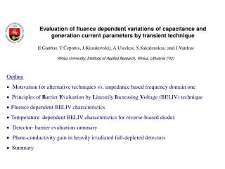
Carrier recombination and emission lifetimes in heavily irradiated pad–detectors and their impact on operational characteristics of pin diodes E.Gaubas1, T.Čeponis1, R.Grigonis2, A.Uleckas1, andJ.Vaitkus1 1Vilnius University, Institute of Applied Research, Vilnius, Lithuania (VU) 2Vilnius University, Laser Research Center, Vilnius, Lithuania (VU) • Outline • Carrier capture (MW-PCD/E) and emission (I-V) lifetime variations • Barrier capacitance variations with fluence (BELIV) • Time and spectral resolved priming of BELIV transients Summary
M=0/en0 Recombination lifetime during and after irradiation After irradiation - wafer and diode samples irradiated by neutrons and protons During protons irradiation/ protons pre-irradiated (MW-PCD) - wafer samples n<n0 recombination prevails - diode samples with applied field n<ni<<n0 Impact of recombination within ENR with R M might be crucial (if n0~1/) on functionality of junction recombination competes with multi-trapping effect
Carrier capture-recombination-generation lifetimes (simple S-R-H approach) rec, gen Generation lifetime EC Without applied E field Recombination lifetime With applied dc E field EV x ni/ND n0 M (EDL-Ei)/kT R>0 G<0 Eqv. Single-type prevailing traps of M=NDL<<n0 at nvn pvp Traps with barriers, multitrapping multi-charge/multi-valency defects • S-R-H is limited by conditions: • M<<n0. then traps are filled by n0 without change in n0; • ii) single type centers dominate • iii) traps do not interact • charge on traps can be ignored relatively to dopants one • Thus, validity of S-R-H conditions should be estimated in applications J.S. Blakemore, in: Semiconductor Statistics, Ch. 8, Pergamon Press, (1962) Traps with exp distributed levels Redistribution of carriers via interaction of traps Photo-, thermo- quenching effects A.Rose. Concepts in photoconductivity and allied problems. Interscience Publishers, John Wiley & Sons, New York-London, 1963.
EC EV x Carrier recombination lifetimes (for M>>n0) Single-species (type) traps Although relaxation to equilibrium/steady-state is kept by M=pM+nM M0, n 0, S-R-H M, M>>n0, S-R-H invalid Capture coefficient <n> should be used instead of v within rigorous analysis n p J.S. Blakemore, in: Semiconductor Statistics, Ch. 8, Pergamon Press, (1962)
Carrier recombination=capture lifetimes (for M>>n0) Only deep slow levels can be filled and observed as carrier emitters Single-species (type) traps X X invalid Space charge generation current Only shallow dopants of proper density are able to support fast operation (w(U)) of a diode ~1/M <1/em to ensure maj. carriers on level are in equilibrium with band Interaction of several type centers appears due to carrier redistribution through bands
Carrier recombination lifetimes for Mi,s>n0 multi-valency(i)/multi-species(s) centers Interaction of the whole system of centers appears due to carrier redistribution through bands, by inter-center recombination (capture-emission) and via charging /configurational transforms of defects System neutrality is supported by free and localized charges/fields. Relaxation is long and complicated. It is similar to the random-walk processes in disordered materials. S.Havlin and D.Ben-Avraham, Advances in physics 51, 187 (2002). L.Pavesi, J. Appl. Phys. 80, 216 (1996). The stretched-exponent model is widely used UCPC =U0exp[–(t/se)] E. Gaubas, S. Juršenas, S. Miasojedovas, J. Vaitkus, and A. Žukauskas JOURNAL OF APPLIED PHYSICS VOLUME 96, NUMBER 8 15 OCTOBER 2004 A single lifetime parameter se can be extracted only when stretched-exponent time scale is employed Relaxation is similar to multi-exponential in any narrow display segment Different techniques may give different lifetime values
Carrier generation/emission lifetime (for M>>n0) Nearly linear reduction of generation lifetime with enhancement of fluence is similar to that of of recombination lifetime characteristic Qualitative emission lifetime dependence on fluence can be estimated from I-V
Examined MW-PCT characteristics imply prevailing of intricate system of defects and reduction of majority carriers. The recombination capture lifetimes become shorter than dielectric relaxation time. • Carrier emission lifetime decrease (increase of leakage current – at UR in I-V),follows capture lifetime reduction (increase of serial resistance R~1/n0 - at UFin I-V), and both manifest a close to a linear decrease with enhancement of fluence Items to clarify: • Whether diode/detector is functional under heavy irradiations? • What is a system of defects and levels, which governs extraction of carriers (UR) and state of material? • Which models are acceptable for prediction of charactreristics? The Barrier Evaluation by Linearly Increasing Voltage (BELIV) transient technique has been employed to clarify, how a reductionof carrier capture lifetime and emission affects junction and material
te Reverse bias BELIV technique Abrupt junction Linearly grade junction
Variations of BELIV transients with temperature and priming by steady-state IRBI as well as dc UF Short carrier capture lifetime reduces n0NDand increases a serial resistanceof ENR. Supply of majority carriers from rear electrode by dc UF priming (due to shrinkage of depletion w width, forward current) restores a junction. Priming by IR illuminationincreases n0 and barrier capacitance observed in BELIV transients restores a junction but enhances leakage current when fast carrier capture/emission is present Reduction of temperature increases (e) and decreases space charge generation current, however,Cb0Cg at UC<0.3 V Combined priming of BELIV transients by temperature reducing(increased e) and by IR illumination (n0)leads to restore of a junction
Barrier capacitance as a function of fluence extracted at 300 K
C-V’s as a function of fluence at 100 kHz and 300 K displacement in barrier capacitance is controlled by (LRC) measurements of phase shift for the ac test signal at fixed frequency in routine C-V Applicability of LRC measured C-V is doubtful for diodes irradiated with >1E13 n/cm2
Barrier partially recovers by n0 priming with IR, dc UF and combined priming with temperature (emission lifetime) decreasing only in diodes irradiated with fluence of <1014 n/cm2. • Short carrier capture and emission times determine low barrier capacitance (capability to to collect charge (transient) at fixed voltage) and large space charge generation (leakage) current in heavily irradiated diodes. • The space charge generation current prevails in heavily irradiated diodes over barrier charging (displacement, which is controlled by measurements of phase shift for the ac test signal in routine C-V), therefore applicability of C-V technique is doubtful for control of heavily irradiated detectors. • Carrier capture and emission lifetimes areshort,and barrier capacitance decreases to geometrical its value at low (U< Ubi) applied voltage of the diodes with enhancement of fluence. Operation of a diode is similar to that of capacitor. • Items to clarify: • Whether diode/detector of the present design is functional after heavy irradiations?- doubtful • What is the system of defects and levels, which governs extraction of carriers (UR) and state of material?- material becomes similar to insulator. • Additonal issues: - if there are filled levels those compensate material; • - how rapidly these levels are able to response to external voltage changes • Which models are acceptable for prediction of characteristics? EC EC EV EV The BELIV technique with spectrally resolved fs pulsed IR (1.1 – 10 µm) biasing has been employed to clarify what is a system of levels and if these levels are filled
mono-polar photoconductivity change of charge state- capacitance Carrier capture rate Variations of BELIV transients by pulsed IR of varied spectrum OPO DFG fs pulse OPO DFG wavelength/quantum for which appears suppression of traps, i.e. recover of BELIV transient of Cb, indicates a system of filled single type deep levels To approve principles structure with known technological defects For qualitative understanding (within depletion approximation): Cb~(ND=n0)1/2~1/w(n0) Cb(t) ~1/M=(en0|tr)/0 (using extended depletion approximation) for transient processes
Variations of BELIV transients by pulsed IR of varied spectrum in neutron irradiated detectors E4 h 0.51eV E3 h 0.41eV E2 h 0.36 eV The shallowest E1 h 0.3 eV
Variations of BELIV transients by pulsed IR of varied spectrum in neutron irradiated detectors The most shallow filled Ered threshold =h 0.5 eV Edeepest -h 1.08eV The most shallowfilled, or a half of two step generation Ered threhold =h 0.52 eV Edeepest -h 1.08eV For 1E14 n/cm2 and h> 0.83 eV possible partial recovering of a barrier, while for h≤ 0.5 eV space charge generation current prevails (rapid capture/emission processes For 1E16 n/cm2 only space charge generation current increases (extremely rapid capture/emission processes) while barrier capacitance is close to Cgeom
A clear structure of deep levels is absent in heavily irradiated diodes >1014 n/cm2 while carriers are generated by inter-band excitation. • Items to clarify: • Whether diode/detector of the present design is functional after heavy irradiations?- doubtful • What is the system of defects and levels, which governs extraction of carriers (UR) and state of material?- material becomes similar to insulator • Additonal issues: - if there are filled levels those compensate material; • - no, high density of various species levels is more probable those are only weakly filled by small n0 • - how rapidly these levels are able to response to external voltage changes • - fast capture of excess carrier and fast space charge generation current response • But system relaxes to equilibrium state very slowly – as estimated from I-V point-by-point measurementsat T<150 K • Which models are acceptable for prediction of characteristics? • The disordered material models-?
Summary • Examined MW-PCT characteristics imply prevailing of intricate system of defects and reduction of majority carriers. The recombination capture lifetimes become shorter than dielectric relaxation time. • Carrier emission lifetime (increase of leakage current – at UR in I-V),follows capture lifetime (increase of serial resistance R~n0 - at UFin I-V) • Barrier capacitance decreases to geometrical value of the diodes with enhancement of fluence. Carrier capture and emission lifetimes are short. The pointed system of deep levels can be revealed only in diodes irradiated with fluence of <1014 n/cm2. • A clear structure of deep levels is absent in heavily irradiated diodes >1014 n/cm2 while carriers can be generated by inter-band excitation.
Thanks to G.Kramberger for neutron irradiations. E.Tuominen, J.Harkonen and J.Raisanen are appreciated for samples (substrates and pin diodes) as well as for proton irradiations. Thank You for attention!
P.Blood and J.W.Orton. The electrical characterization of semiconductors: majority carriers and electron states, (Academic Press, London –San Diego-New York, 1992). tr Depletion aproximation for material containing only dopants: Limitations: for steady-state only numerical integration assumption for transients gives depletion approximation
Transient currents in depletion region in deep traps containing material tr Test harmonic signal Uac<kT/e, to evaluate Cb,, by control of phase shift avoiding xd>tr , i.e. desirable regime EC(x)-EC(xd)<kT. P.Blood and J.W.Orton. The electrical characterization of semiconductors: majority carriers and electron states, (Academic Press, London –San Diego-New York, 1992).