Quantum Confinement
Quantum Confinement. Overview of Quantum Confinement. History : In 1970 Esaki & Tsu proposed fabrication of an artificial structure, which would consist of alternating layers of 2 different semiconductors with Layer Thickness 1 nm = 10 Å = 10 -9 m SUPERLATTICE


Quantum Confinement
E N D
Presentation Transcript
Overview of Quantum Confinement History: In 1970 Esaki & Tsu proposed fabrication of an artificial structure, which would consist of alternating layers of 2 different semiconductors with Layer Thickness 1 nm = 10 Å = 10-9 mSUPERLATTICE • PHYSICS:The main idea was that introduction of an artificial periodicity will “fold” the Brillouin Zones into smaller BZ’s “mini-zones”. The idea was that this would raise the conduction band minima, which was needed for some device applications.
Modern growth techniques (starting in the 1980’s), especially MBE & MOCVD, make fabrication of such structures possible! • For the same reason, it is also possible to fabricatemany other kindsof artificial structures on the scale of nm (nanometers) “Nanostructures” Superlattices = “2 dimensional” structures Quantum Wells = “2 dimensional”structures Quantum Wires = “1 dimensional”structures Quantum Dots = “0 dimensional” structures!! • Clearly, it is not only the electronic properties of materials which can be drastically altered in this way. Also, vibrational properties (phonons). Here, only electronic properties & only an overview! • For many years, quantum confinement has been a fast growing field in both theory & experiment! It is at the forefront of current research! • Note that I am not an expert on it!
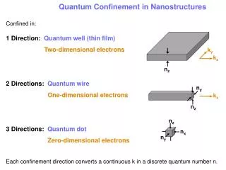
ky kx nz ny kx nz nz nx ny Quantum Confinement in Nanostructures: Overview Electrons Confined in 1 Direction:Quantum Wells(thin films): Electrons can easily move in2 Dimensions! Electrons Confined in 2 Directions: Quantum Wires: Electrons can easily move in1 Dimension! Electrons Confined in 3 Directions:Quantum Dots: Electrons can easily move in0 Dimensions! Each further confinement direction changes a continuous k component to a discrete component characterized by a quantum number n. 1 Dimensional Quantization! 2 Dimensional Quantization! 3 Dimensional Quantization!
PHYSICS:Back to the bandstructure chapter: • Consider the 1st Brillouin Zone for the infinite crystal.The maximum wavevectors are of the order km (/a) a = lattice constant. The potentialV is periodic with period a. In the almost free e- approximation, the bands are free e- like except near the Brillouin Zone edge. That is, they are of the form: E (k)2/(2mo) So, the energy at the Brillouin Zone edge has the form: Em (km)2/(2mo) or Em ()2/(2moa2)
PHYSICS • SUPERLATTICES Alternating layers of material. Periodic, with periodicityL(layer thickness). Let kz =wavevector perpendicular to the layers. • In a superlattice, the potential Vhas a new periodicity in the z direction with periodicity L >> a In the z direction, the Brillouin Zone is much smaller than that for an infinite crystal. The maximum wavevectors are of the order: ks (/L) At the BZ edge in the z direction, the energy has the form: Es ()2/(2moL2) + E2(k) E2(k) =the 2 dimensional energy fork in the x,y plane. Note that:()2/(2moL2) << ()2/(2moa2)
Primary Qualitative Effects of Quantum Confinement • Consider electrons confined along 1 direction(say, z) to a layer of width L: Energies • The energy bands are quantized (instead of continuous) in kz& shifted upward. So kz is quantized: kz = kn = [(n)/L], n = 1, 2, 3 • So, in the effective mass approximation (m*),the bottom of the conduction band is quantized(like a particle in a 1 d box)& shifted: En = (n)2/(2m*L2) • Energies are quantized!Also, thewavefunctions are 2 dimensional Bloch functions(traveling waves)for kin the x,yplane &standing waves in the z direction.
Quantum Confinement Terminology Quantum Well QW = A single layer of material A (layer thickness L), sandwiched between 2 macroscopically large layers of material B. Usually, the bandgaps satisfy: EgA < EgB Multiple Quantum Well MQW =Alternating layers of materials A(thickness L) & B(thickness L). In this case: L >> L So, the e- & e+ in one Alayer are independent of those in other Alayers. Superlattice SL =Alternating layers of materials A& B with similar layer thicknesses.
Brief Elementary Quantum Mechanics & Solid State Physics Review • Quantum Mechanicsof a Free Electron: • The energies are continuous: E = (k)2/(2mo) (1d, 2d, or 3d) • The wavefunctions are traveling waves: ψk(x) = A eikx(1d)ψk(r) = A eikr(2d or 3d) • Solid State Physics:Quantum Mechanics of an Electron in a Periodic Potential in an infinite crystal : • The energy bands are (approximately)continuous: E= Enk • At the bottom of the conduction band or the top of the valence band, in the effective mass approximation, the bands can be written: Enk (k)2/(2m*) • The wavefunctions are Bloch Functions = traveling waves: Ψnk(r) = eikrunk(r); unk(r) = unk(r+R)
Some Basic Physics • Density of states (DoS) in 3D:
QM Review: The 1d (infinite) Potential Well(“particle in a box”)In all QM texts!! • We want to solve the Schrödinger Equation for: x < 0, V ; 0 < x < L, V = 0; x > L, V -[2/(2mo)](d2 ψ/dx2) = Eψ • Boundary Conditions: ψ = 0at x = 0 & x = L (V there) • Energies: En = (n)2/(2moL2), n = 1,2,3 Wavefunctions: ψn(x) = (2/L)½sin(nx/L) (a standing wave!) Qualitative Effects of Quantum Confinement: Energies are quantized & ψchanges from a traveling wave to a standing wave.
In 3Dimensions… • For the 3D infinite potential well: R Real Quantum Structures aren’t this simple!! • In Superlattices & Quantum Wells,the potential barrier is obviously not infinite! • In Quantum Dots, there is usually ~ spherical confinement, not rectangular. • The simple problem only considers a single electron. But, inreal structures, there are many electrons& alsoholes! • Also, there is oftenan effective mass mismatchat the boundaries.That isthe boundary conditions we’ve used are too simple!
QM Review: The 1d (finite) Rectangular Potential Well In most QM texts!! Analogous to a Quantum Well • We want to solve the Schrödinger Equation for: [-{ħ2/(2mo)}(d2/dx2) + V]ψ = εψ (εE) V = 0, -(b/2) < x < (b/2); V = Vo otherwise We want bound states:ε < Vo
(½)b -(½)b Vo Solve the Schrödinger Equation: [-{ħ2/(2mo)}(d2/dx2) + V]ψ = εψ (εE) V = 0, -(b/2) < x < (b/2) V = Vo otherwise Bound states are in Region II Region II: ψ(x) is oscillatory Regions I & III: ψ(x) is decaying V= 0
The 1d (finite) rectangular potential wellA brief math summary! Define:α2 (2moε)/(ħ2); β2 [2mo(ε - Vo)]/(ħ2) The Schrödinger Equation becomes: (d2/dx2) ψ + α2ψ = 0, -(½)b < x < (½)b (d2/dx2) ψ - β2ψ = 0, otherwise. Solutions: ψ = C exp(iαx) + D exp(-iαx), -(½)b < x < (½)b ψ = A exp(βx), x < -(½)b ψ = A exp(-βx), x > (½)b Boundary Conditions: ψ & dψ/dx are continuous SO:
Algebra (2 pages!)leads to: (ε/Vo) = (ħ2α2)/(2moVo) ε, α, β are related to each other by transcendental equations. For example: tan(αb) = (2αβ)/(α2- β2) • Solve graphically or numerically. • Get:Discrete Energy Levels in the well (a finite number of finite well levels!)
Vo • Even eigenfunctionsolutions (a finite number): Circle,ξ2 + η2 = ρ2, crosses η = ξ tan(ξ) o o b
Vo b • Odd eigenfunction solutions: Circle,ξ2 + η2 = ρ2, crossesη = -ξ cot(ξ) |E2| < |E1| o o b
ky kx nz ny kx nz nz nx ny Quantum Confinement in Nanostructures Confined in: 1 Direction: Quantum well (thin film) Two-dimensional electrons 2 Directions: Quantum wire One-dimensional electrons 3 Directions: Quantum dot Zero-dimensional electrons Each confinement direction converts a continuous k in a discrete quantum number n.
E d Electron Scattering EVacuum Inverse Photoemission EFermi Photoemission 0 /d k /a = zone boundary Quantization in a Thin Crystal An energy band with continuous k is quantized into N discrete points knin a thin film withN atomic layers. n = 2d/n kn = 2/n = n /d N atomic layers with the spacing a = d/n N quantized states with kn≈ n/d (n=1,…,N)
Quantization in Thin Graphite Films layers = graphite E Lect.7b, Slide11 1 layer = graphene 2 layers EVacuum EFermi 3 layers Photoemission 0 /d k /a 4 layers N atomic layers with spacing a = d/n : N quantized states with kn≈ N /d
becoming continuous for N Quantum Well States in Thin Films discrete for small N Paggel et al. Science 283, 1709 (1999)
n n Counting Quantum Well States Periodic Fermi level crossing of quantum well states with increasing thickness Number of monolayers N
n 6 5 4 3 2 1 Quantum Well Oscillations in Electron Interferometers Fabry-Perot interferometer model: Interfaces act like mirrors for electrons. Since electrons have so short wavelengths, the interfaces need to be atomically precise. Himpsel Science 283, 1655 (1999) Kawakami et al. Nature 398, 132 (1999)
The Important Electrons in a Metal • Energy EFermi • Energy Spread 3.5 kBT • Transport (conductivity, magnetoresistance, screening length, ...) • Width of the Fermi function: • FWHM 3.5 kBT • Phase transitions (superconductivity, magnetism, ...) • Superconducting gap: • Eg 3.5 kBTc (Tc= critical temperature)
Energy Bands of Ferromagnets Calculation Photoemission data Ni Energy Relative to EF [eV] 0.7 0.9 1.1 k|| along [011] [Å-1 ] States near the Fermi level cause the energy splitting between majority and minority spin bands in a ferromagnet (red and green).
Quantum Well States and Magnetic Coupling The magnetic coupling between layers plays a key role in giant magnetoresistance (GMR), the Nobel prize winning technology used for reading heads of hard disks. This coupling oscillates in sync with the density of states at the Fermi level. (Qiu, et al. PR B ‘92)
Spin-Polarized Quantum Well States Magnetic interfaces reflect the two spins differently, causing a spin polarization. Minority spins discrete, Majority spins continuous
Giant Magnetoresistance and Spin - Dependent Scattering Parallel Spin Filters Resistance Low Opposing Spin Filters Resistance High • Filtering mechanisms • Interface: Spin-dependent Reflectivity Quantum Well States • Bulk: Spin-dependent Mean Free Path Magnetic “Doping”
Magnetoelectronics Spin currents instead of charge currents Magnetoresistance = Change of the resistance in a magnetic field Giant Magnetoresistance (GMR): (Metal spacer, here Cu) Tunnel Magnetoresistance (TMR): (Insulating spacer, MgO)
ELEC 7970 Special Topics on Nanoscale Science and Technology Quantum Wells, Nanowires, and Nanodots Summer 2003 Y. Tzeng ECE Auburn University
Quantum confinement • Trap particles and restrict their motion • Quantum confinement produces new material behavior/phenomena • “Engineer confinement”- control for specific applications • Structures • Quantum dots (0-D) only confined states, and no freely moving ones • Nanowires (1-D) particles travel only along the wire • Quantum wells (2-D) confines particles within a thin layer http://www.me.berkeley.edu/nti/englander1.ppt http://phys.educ.ksu.edu/vqm/index.html (Scientific American)
Figure 11: Energy-band profile of a structure containing three quantum wells, showing the confined states in each well. The structure consists of GaAs wells of thickness 11, 8, and 5 nm in Al0.4 Ga0.6 As barrier layers. The gaps in the lines indicating the confined state energies show the locations of nodes of the corresponding wavefunctions. Quantum well heterostructures are key components of many optoelectronic devices, because they can increase the strength of electro-optical interactions by confining the carriers to small regions. They are also used to confine electrons in 2-D conduction sheets where electron scattering by impurities is minimized to achieve high electron mobility and therefore high speed electronic operation. http://www.utdallas.edu/~frensley/technical/hetphys/node11.html#SECTION00050000000000000000 http://www.utdallas.edu/~frensley/technical/hetphys/hetphys.html
http://www.evidenttech.com/pdf/wp_biothreat.pdf http://www.evidenttech.com/why_nano/why_nano.php
February 2003The Industrial Physicist Magazine Quantum Dots for Sale Nearly 20 years after their discovery, semiconductor quantum dots are emerging as a bona fide industry with a few start-up companies poised to introduce products this year. Initially targeted at biotechnology applications, such as biological reagents and cellular imaging, quantum dots are being eyed by producers for eventual use in light-emitting diodes (LEDs), lasers, and telecommunication devices such as optical amplifiers and waveguides. The strong commercial interest has renewed fundamental research and directed it to achieving better control of quantum dot self-assembly in hopes of one day using these unique materials for quantum computing. Semiconductor quantum dots combine many of the properties of atoms, such as discrete energy spectra, with the capability of being easily embedded in solid-state systems. "Everywhere you see semiconductors used today, you could use semiconducting quantum dots," says Clint Ballinger, chief executive officer of Evident Technologies, a small start-up company based in Troy, New York... http://www.evidenttech.com/news/news.php
Quantum Dots for SaleThe Industrial Physicist reports that quantum dots are emerging as a bona fide industry. Evident NanocrystalsEvident's nanocrystals can be separated from the solvent to form self-assembled thin films or combined with polymers and cast into films for use in solid-state device applications. Evident's semiconductor nanocrystals can be coupled to secondary molecules including proteins or nucleic acids for biological assays or other applications. http://www.evidenttech.com/why_nano/docs.php http://www.evidenttech.com/index.php
EviArrayCapitalizing on the distinctive properties of EviDots™, we have devised a unique and patented microarray assembly. The EviArray™ is fabricated with nanocrystal tagged oligonucleotide probes that are also attached to a fixed substrate in such a way that the nanocrystals can only fluoresce when the DNA probe couples with the corresponding target genetic sequence. http://www.evidenttech.com/why_nano/docs.php
EviDots - Semiconductor nanocrystalsEviFluors- Biologically functionalized EviDotsEviProbes- Oligonucleotides with EviDotsEviArrays- EviProbe-based assay system Optical Transistor- All optical 1 picosecond performanceTelecommunications- Optical Switching based on EviDotsEnergy and Lighting- Tunable bandgap semiconductor
Why nanowires? “They represent the smallest dimension for efficient transport of electrons and excitons, and thus will be used as interconnects and critical devices in nanoelectronics and nano-optoelectronics.” (CM Lieber, Harvard) General attributes & desired properties • Diameter – 10s of nanometers • Single crystal formation -- common crystallographic orientation along the nanowire axis • Minimal defects within wire • Minimal irregularities within nanowire arrays http://www.me.berkeley.edu/nti/englander1.ppt
Nanowire fabrication • Challenging! • Template assistance • Electrochemical deposition • Ensures fabrication of electrically continuous wires since only takes place on conductive surfaces • Applicable to a wide range of materials • High pressure injection • Limited to elements and heterogeneously-melting compounds with low melting points • Does not ensure continuous wires • Does not work well for diameters < 30-40 nm • CVD • Laser assisted techniques http://www.me.berkeley.edu/nti/englander1.ppt
Magnetic nanowires • Important for storage device applications • Cobalt, gold, copper and cobalt-copper nanowire arrays have been fabricated • Electrochemical deposition is prevalent fabrication technique • <20 nm diameter nanowire arrays have been fabricated Cobalt nanowires on Si substrate (UMass Amherst, 2000) http://www.me.berkeley.edu/nti/englander1.ppt
Silicon nanowire CVD growth techniques • With Fe/SiO2 gel template (Liu et al, 2001) • Mixture of 10 sccm SiH4 & 100 sccm helium, 5000C, 360 Torr and deposition time of 2h • Straight wires w/ diameter ~ 20nm and length ~ 1mm • With Au-Pd islands (Liu et al, 2001) • Mixture of 10 sccm SiH4 & 100 sccm helium, 8000C, 150 Torr and deposition time of 1h • Amorphous Si nanowires • Decreasing catalyst size seems to improve nanowire alignment • Bifurcation is common • 30-40 nm diameter and length ~ 2mm http://www.me.berkeley.edu/nti/englander1.ppt
Template assisted nanowire growth • Create a template for nanowires to grow within • Based on aluminum’s unique property of self organized pore arrays as a result of anodization to form alumina (Al2O3) • Very high aspect ratios may be achieved • Pore diameter and pore packing densities are a function of acid strength and voltage in anodization step • Pore filling – nanowire formation via various physical and chemical deposition methods http://www.me.berkeley.edu/nti/englander1.ppt
Al2O3 template preparation • Anodization of aluminum • Start with uniform layer of ~1mm Al • Al serves as the anode, Pt may serve as the cathode, and 0.3M oxalic acid is the electrolytic solution • Low temperature process (2-50C) • 40V is applied • Anodization time is a function of sample size and distance between anode and cathode • Key Attributes of the process (per M. Sander) • Pore ordering increases with template thickness – pores are more ordered on bottom of template • Process always results in nearly uniform diameter pore, but not always ordered pore arrangement • Aspect ratios are reduced when process is performed when in contact with substrate (template is ~0.3-3 mm thick) http://www.me.berkeley.edu/nti/englander1.ppt
The alumina (Al2O3) template (T. Sands/ HEMI group http://www.mse.berkeley.edu/groups/Sands/HEMI/nanoTE.html) alumina template Si substrate http://www.me.berkeley.edu/nti/englander1.ppt 100nm (M. Sander)
Bi2Te3 nanowire unfilled pore alumina template Electrochemical deposition • Works well with thermoelectric materials and metals • Process allows to remove/dissolve oxide barrier layer so that pores are in contact with substrate • Filling rates of up to 90% have been achieved http://www.me.berkeley.edu/nti/englander1.ppt (T. Sands/ HEMI group http://www.mse.berkeley.edu/groups/Sands/HEMI/nanoTE.html)
Template-assisted, Au nucleated Si nanowires • Gold evaporated (Au nanodots) into thin ~200nm alumina template on silicon substrate • Ideally reaction with silane will yield desired results • Need to identify equipment that will support this process – contamination, temp and press issues • Additional concerns include Au thickness, Au on alumina surface, template intact vs removed Au dots Au 100nm 1µm http://www.me.berkeley.edu/nti/englander1.ppt template (top) (M. Sander)
Nanometer gap between metallic electrodes Before breaking SET with a 5nm CdSe nanocrystal After breaking Electromigration caused by electrical current flowing through a gold nanowire yields two stable metallic electrodes separated by about 1nm with high efficiency. The gold nanowire was fabricated by electron-beam lithography and shadow evaporation. http://www.lassp.cornell.edu/lassp_data/mceuen/homepage/Publications/EMPaper.pdf
Quantum and localization of nanowire conductance • Nanoscale size exhibits the following properties different from those found in the bulk: • quantized conductance in point contacts and narrow channels whose characteristics (transverse) dimensions approach the electronic wave length • Localization phenomena in low dimensional systems • Mechanical properties characterized by a reduced propensity for creation and propagation of dislocations in small metallic samples. • Conductance of nanowires depend on • the length, • lateral dimensions, • state and degree of disorder and • elongation mechanism of the wire. http://dochost.rz.hu-berlin.de/conferences/conf1/PDF/Pascual.pdf