Download
1 / 31
310 likes | 542 Vues
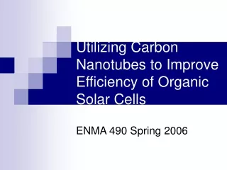
Utilizing Carbon Nanotubes to Improve Efficiency of Organic Solar Cells. ENMA 490 Spring 2006. Motivation. Problem: Lack of power in remote locations Possible solution: Organic solar cells are less expensive and more portable than conventional solar cells Main issue: Inadequate efficiency.

E N D
Utilizing Carbon Nanotubes to Improve Efficiency of Organic Solar Cells ENMA 490 Spring 2006
Motivation • Problem: Lack of power in remote locations • Possible solution: Organic solar cells are less expensive and more portable than conventional solar cells • Main issue: Inadequate efficiency
What We Did • Focus: Increase the efficiency through the addition of carbon nanotubes • Research Goal: Model a basic device and propose an ideal structure for more efficient power generation • Experimental Goal: Build selected devices to test parameters
Research Team Erik Lowery Nathan Fierro Adam Haughton Richard Elkins Project Organization Experimental Team Erin Flanagan Scott Wilson Matt Stair Michael Kasser
How Organic Solar Cells Work • Photon absorption, excitons are created • Excitons diffusion to an interface • Charge separation due to electric fields at the interface. • Separated charges travel to the electrodes. High Work Function Electrode Donor Material E Acceptor Material Low Work Function Electrode
Critical Design Issues • Exciton creation via photon absorption • Material absorption characteristics • Exciton diffusion to junction • Interfaces within exciton diffusion length (nanoscale structure) • Charge separation • Donor/Acceptor band alignment • Transport of charge to electrodes • High charge mobility
The Active Layer • Composed of an electron donor and electron acceptor • 3 types of junctions • Bilayer • Diffuse Bilayer • Bulk heterojunction • Usually the excitons from the electron donor are responsible for the photocurrent
Electron Acceptor • MEH-PPV-CN • Electron acceptor • CN group • Increased band alignment • Higher electron affinity • Electrical Properties • Poor charge mobility • Optical Properties • Peak emission at 558 nm • Peak absorption at 405 nm (~3eV) Solar Spectrum MEH-PPV-CN Irradiance (W/m^2) Absorption (arb. Units) Energy, eV
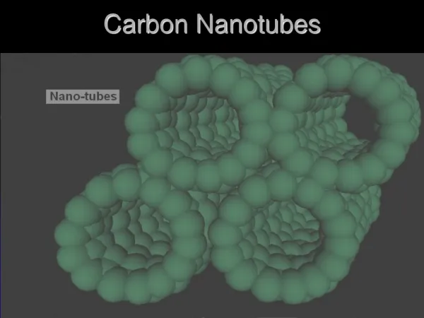
Electron Donor • Carbon Nanotubes • Orders of magnitude better conductance than polymers • Our nanotubes specifications (Zyvex) • Functionalized • Diameter: 5-15 nm • Length: 0.5-5 microns • MWNT (60% metallic 40% semiconducting) AFM Amplitude Scan
Electron Donor (cont.) • Carbon Nanotubes • Optical Properties • Diameter • SW vs. MW • Chirality (Semi-conducting vs metallic)
Modeling • Model Geometry • Photogeneration of Excitons • Exciton Transport to Junction • Electron Hole Separation • Charge Transport to Electrode
Model Geometry Incoming Light X=0 X=L ITO CNT MEH-PPV-CN Al Define A to be the area perpendicular to the incoming light.
Photogeneration of Excitons • Start with Beer-Lambert absorption equation: • Arrive at expression for # Photons absorbed per unit area, per unit time • Use either blackbody approximation or numerical data for the solar spectrum (Sinc)
Exciton Transport to Junction • Diffusion Model • Initial and Boundary Conditions Decay Term, simple time-dependent model Source Term, accounts for exciton generation Diffusion Term Excitons destroyed at CNT/Electrode Interface Excitons destroyed at CNT/Polymer Junction Initially, assume ground state, no excitons anywhere.
Charge Transport to Electrode • Holes move along CNTs • Hole Mobility ~ 3000 cm2/Vs • Electrons move along MEH-PPV-CN • Electron Mobility ~ 3.3x10⁻⁷ cm2/Vs • Current density is directly related to mobility; Increased mobility leads to higher current densities.
Modeling Summary • CNT/MEH-PPV junctions within diffusion length of exciton generation points • Thickness Optimization Problem: • Maximizing thickness gives more excitons • Minimizing thickness leads to higher current
Ideal Structure ITO Nanotubes Nanoscale mixing MEH-PPV-CN Al Nanoscale mixing allows excitons to charge separate before they recombine Structure allows for the bulk heterojunction and minimizes the travel distance to the electrodes
Experimental Design • Experimental design parameters • CNT concentration • Method of mixing • Spin Parameters • Solvents
Device Process Flow ITO .4 mm .7 mm 2.5 mm .2 mm
Device Process Flow PEDOT ~100nm Al contacts ~600 Å
Device Process Flow LiF ~ 20 Å Al contacts
Experimental Results Pure polymer devices acted like diodes. Light emission was observed at higher currents (8 mA)
Experimental Results Pure CNT acted like a resistor, R >350Ω.
Experimental Design Issues We Addressed • Nanotube Processing • Method of dispersion • Type of solvent • Concentration CNT • amount of CNT in solvent • CNT to Polymer • Diffused junction vs. bulk heterojunction
Results Summary • Absorption spectra measured • AFM to check spatial distribution of nanotubes • No successful devices made • Possible causes: • CNT shorting • Functionalized CNTs might be a problem
Conclusions • Experimental: • Device process recipe needs to be refined • Solve experimental design problems to work on successful device • Modeling: • Diffusion model considerations point towards improving efficiency by creating nanoscale structure • Need to consider charge transport in more detail
Acknowledgements • We would like to thank the following people/organizations: • Dr. Gary Rubloff • Dr. Danilo Romero • Laboratory for Physical Sciences • Zyvex