Download
1 / 50
500 likes | 534 Vues
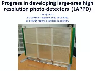
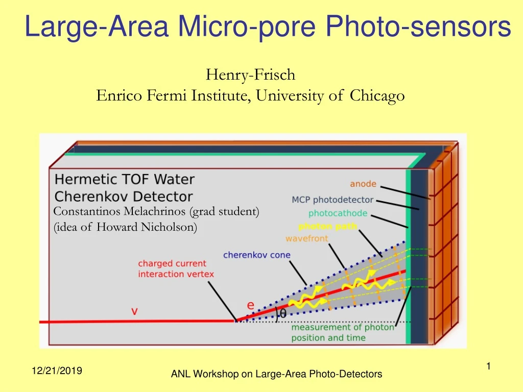
Explore the potential of large-area micro-pore photo-sensors for diverse applications, from Cherenkov counters to neutrino detectors. Discuss scalability, cost-effectiveness, and performance expectations. Investigate opportunities for enhanced detector robustness and improved signal determination in challenging conditions. ANL Workshop on Large-Area Photo-Detectors.

E N D
Large-Area Micro-pore Photo-sensors Henry-Frisch Enrico Fermi Institute, University of Chicago Constantinos Melachrinos (grad student) (idea of Howard Nicholson) ANL Workshop on Large-Area Photo-Detectors
Large-Area Micro-pore Photo-sensorsOUTLINE • Basic ideas- small characteristic size, homogeneity, scalability, integrated low-power cheap electronics. • Parameters tuneable to application- space/time resolution, occupancy, readout deadtime, cost. • Status and proposed time-line for development? • Typical expected performance • Application to a water Cherenkov counter (also to Liquid Argon?) • Possible Opportunities: • `Hermetic’- close to 100% coverage? • Reduced cost of PM’s for same volume • More opportunities for cavern aspect ratio/ fiducial volume • Robustness against pressure, magnetic field? • Tracking detector- possible track/vertex reconstruction? • Sign determination (weak field)?? ANL Workshop on Large-Area Photo-Detectors
Large-Area Micro-pore Photo-sensorsWHAT THIS IS NOT A proposal for an alternative to the baseline detector A mature collection of thoughts A description of a well-understood technology A plan with a schedule and resource requirements Any attempt to get in the way of making DUSEL real. WHAT THIS IS A response to new R&D on large-area psec photo-detectors started for collider applications and PET, and enabled by new developments in front-end electronics. An investigation into a possible application of large-area fast photo-detectors to a high-priority US project. An exploration of the parameter space for water Cherenkov neutrino detectors- coverage, resolution,.. An effort that would have a lot of spin-offs for society. ANL Workshop on Large-Area Photo-Detectors
Typical path lengths for light and electrons are set by physicaldimensions of the light collection and amplifying device. Why has 100 psec been the # for 60 yrs? These are now on the order of an inch. One inch is 100 psec. That’s what we measure- no surprise! (pictures from T. Credo) Typical Light Source (With Bounces) Typical Detection Device (With Long Path Lengths) ANL Workshop on Large-Area Photo-Detectors
RF Transmission Lines as anodes • Small features for amplification- `Homogeneous’ • Large transverse size for readout is pulse shape-preserving • Readout both ends of transmission lines • Work on leading edge- ringing not a problem for this fine segmentation Solving the Small/large Problem ANL Workshop on Large-Area Photo-Detectors
Characteristics we need • Feature size <~ 300 microns (= 1 psec at c) • Homogeneity (ability to make uniform large-area- think amorphous semicndtr solar-panel) • Fast rise-time and/or constant signal shape • Lifetime/robustness/simplicity • Cost/unit-area << that for photo-multipliers ANL Workshop on Large-Area Photo-Detectors
An Explanation of what follows • I’ve been driven by wanting to follow flavor-flow in colliders- most of our work has been focused on that geometry- light made in window by a relativistic particle, ~30 photo-electrons, goal of <= 1 psec timing. You’ll see most results for this regime- have to scale back to single photons • Haven’t thought much at all about applying this to neutrino detectors- Howard Nicholson suggested it while listening to a talk. Hence this workshop. • Note- good time and space resolution come naturally in this design- get 3D (`tomographic’) info by design. ANL Workshop on Large-Area Photo-Detectors
Detector Development- 3 Prongs • 1. Electronics- have settled on wave-form sampling Already demonstrated by Breton, Delanges,Ritt, and Varner- many `pieces’ exist, main change is going to faster process and pooling expertise. Reasonable precision (see talk at Lyon by Genat)- few psec with present rise times, ~1 with faster MCP design. Gives much more than time- space, pileup, etc. (Tang Lyon talk) 2. MCP development- techniques and facilities (probably) exist- ALD, anodic alumina--will require industry, natl labs, 3. Simulation – Electronics simulation in good shape Rudimentary `end-to-end’ MCP device simulation exists- starting up with commercial packages (SimIon, CPO, …) Validation with laser teststand and beam line started ANL Workshop on Large-Area Photo-Detectors
GOAL: to Develop Large-Area Photo-detectors with Psec Time and mm SpaceResolution Too small- can go larger- (But how does multiplication work- field lines?) From Argonne MSD ALD web page- can we make cheap (relatively) ultra-fast planar photo-detector modules? ANL Workshop on Large-Area Photo-Detectors
Generating the signal for relativistic particles (HEP, nuclear, astro, accelerator- but different for neutrinos) Incoming rel. particle Custom Anode Present work is with commercial MCP’s: e.g. Burle/Photonis Planicons. Expensive (!), hard to get, little flexibility. BUT- it works. And well. Use Cherenkov light - fast ANL Workshop on Large-Area Photo-Detectors
Design Goals Colliders: ~ 1 psec resolution, < 100K$/m2 Neutrino H2O: ~100 psec resolution, < 1K$/m2 PET: ~ 30 psec resolution, < 20% of crystal cost Micro-photograph of Burle 25 micron tube- Greg Sellberg (Fermilab)- ~2M$/m2- not including readout ANL Workshop on Large-Area Photo-Detectors
Proof of Principle • Camden Ertley results using ANL laser-test stand and commercial Burle 25-micron tube- lots of photons • (note- pore size may matter less than current path!- we can do better with ALD custom designs (transmission lines)) ANL Workshop on Large-Area Photo-Detectors
Understanding the contributing factors to 6 psec resolutions with present Burle/Photonis/Ortec setups- Jerry Vavra’s Numbers • TTS: 3.8 psec (from a TTS of 27 psec) • Cos(theta)_cherenk 3.3 psec • Pad size 0.75 psec • Electronics 3.4 psec ANL Workshop on Large-Area Photo-Detectors
`Photo-multiplier in a Pore’ • Idea is to build a PMT structure inside each pore- have a defined dynode chain of rings of material with high secondary emissivity so that the start of the shower has a controlled geometry (and hence small TTS) • One problem is readout- how do you cover a large area and preserve the good timing? • Proposed solution- build anode into pores, capacitively couple into transmission lines to preserve pulse shape. ANL Workshop on Large-Area Photo-Detectors
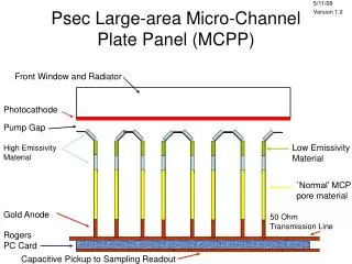
Psec Large-area Micro-Channel Plate Panel (MCPP)- LDRD proposal to ANL (with Mike Pellin/MSD) N.B.- this is a `cartoon’- working on workable designs-join us… Front Window and Radiator Photocathode Pump Gap Low Emissivity Material High Emissivity Material `Normal’ MCP pore material Gold Anode 50 Ohm Transmission Line Rogers PC Card ANL Workshop on Large-Area Photo-Detectors Capacitive Pickup to Sampling Readout
Get position AND timeAnode Design and Simulation(Fukun Tang) • Transmission Line- readout both ends=> pos and time • Cover large areas with much reduced channel account. ANL Workshop on Large-Area Photo-Detectors
Photonis Planicon on Transmission Line Board Couple 1024 pads to strip-lines with silver-loaded epoxy (Greg Sellberg, Fermilab). ANL Workshop on Large-Area Photo-Detectors
Photonis Planicon on Transmission Line Board Ed May, Jean-Francois Genat- a week ago… Left: laser on one spot; Right: laser then moved over 10 mm and plots superposed. (3.1 psec/count- last week) ANL Workshop on Large-Area Photo-Detectors
Comparison of measurements (Ed May and Jean-Francois Genat and simulation (Fukun Tang) • Transmission Line- simulation shows 3.5GHz bandwidth- 100 psec rise (well-matched to MCP) • The time difference yields a velocity of 64ps/cm against 68ps predicted
Scaling Performance to Large AreaAnode Simulation(Fukun Tang) • 48-inch Transmission Line- simulation shows 1.1 GHz bandwidth- still better than present electronics. ANL Workshop on Large-Area Photo-Detectors
Front-end Electronics Critical path item- probably the reason psec detectors haven’t been developed • We had started with very fast BiCMOS designs- IBM 8HP-Tang designed two (really pretty) chips • Realized that they are too power-hungry and too ‘boutique’ for large-scale applications • Have been taught by Gary Varner, Stefan Ritt, Eric DeLanges, and Dominique Breton that there’s a more clever and elegant way- straight CMOS – sampling onto an array of capacitors • Have formed a collaboration to do this- have all the expert groups involved (formal with Hawaii and France)- see talks by Tang and Jean-Francois at Lyon ANL Workshop on Large-Area Photo-Detectors
FY-08 Funds –ChicagoAnode Design and Simulation(Fukun Tang) ANL Workshop on Large-Area Photo-Detectors
Front-end Electronics • Wave-form sampling does well- CMOS (!) ANL Workshop on Large-Area Photo-Detectors
Front-end Electronics- Schedule • Collaboration with ANL, UC,Hawaii, Orsay, Saclay, and advise and wisdom and parts from PSI => have all 4 sampling groups. J-F in France now with them. • Have proposed 3 ½ year schedule for completion of 0.13 micron 40-GS/sec ASIC for collider and other relativistic particle applications. • Present chips probably adequate for neutrino application- don’t need few psec resolution- have new PSI DRS4 on its way to UC now; chips from all gps in use in running experiments • Needs a needs assessment- but no show stoppers... ANL Workshop on Large-Area Photo-Detectors
Modus Operandi so far • In Nov. 2005, we had our 1st workshop- idea was to invite folks working or interested in related subjects- didn’t know many (most) of them • Have developed tools and knowledge- also contact with pioneers and practictioners (Ohshima, Howorth, Va’vra,…; Breton, Delanges, Ritt, Varner) • Development clearly too big for one group- devices, electronics, applications- have worked collaboratively with each other, national labs (see talks by Karen, Andrew,Jerry,…), and industry (Burle/Photonis, Photek, IBM,…) ANL Workshop on Large-Area Photo-Detectors
Development of the Device • Started effort with ANL HEP, Materials Science, and Energy Systems Divisions • Have started investigating AAO using facilities of Center for Nano-scale Materials Hau Wang (ANL/MSD) First try- not final pores or final process… but shows what they can do quick.. ANL Workshop on Large-Area Photo-Detectors
Development of the Device • Schedule- working on making a resource-loaded schedule • Workshop at end of February dedicated to device development • Idea is to have a preliminary plan by end of workshop real plan by early summer • Do relativistic particle, single-photon, and PET in parallel until paths diverge. • My hope is that it’s 3-4 years. ANL Workshop on Large-Area Photo-Detectors
Application to a water Cherenkov Counter- effect on the physics ANL Workshop on Large-Area Photo-Detectors
Application to a water Cherenkov Counter- effect on the physics • What does coverage buy ? • What does spatial resolution in x-y buy? • Can x-y-z resolution allow track reconstruction? • Can x-y-z resolution allow pizero-electron sep? • Can one get momentum from multiple scattering? • What are the trade-offs in geometry if you have robust (pressure-resistant) detectors? (Mayly) • What haven’t we thought of? (e.g. magnetic field for sign determination). ANL Workshop on Large-Area Photo-Detectors
Schedule and Milestones (?) • Small (1”) AAO with pores- started (Hau) • Same with ALD- tests of gain • Same with photo-cathode and anode- laser tests • 2” x 6” AAO with pores • Same with ALD- tests of gain • Same with photo-cathode and anode • Same with sampling chip readout (chip started) • 8” x 8” (or so- a “floor-tile”)- same steps • In parallel of latter, commercialization (NDA signed). • 4 years??? Depends on talent, resources, investment- many details- but many indications it’s possible. ANL Workshop on Large-Area Photo-Detectors
Thank you ANL Workshop on Large-Area Photo-Detectors
My Questions This Time-INote- many questions from previous workshops have been answered! • What is the electric field geometry in the MCP pore? (what are bulk and surface resistivities? ). • What is the response of a nano-carbon film to 200 eV electrons? (photons?) • After the first strike, can the pore be straight? • If one uses diamond (e.g.), do you really need fewer strikes? ANL Workshop on Large-Area Photo-Detectors
My Questions This Time-IINote- many questions from previous workshops have been answered! • Other ways to make pores- e.g. Pierre Jarron’s developments? • Who makes big photocathodes? (Pioneer?) • Who is interested in learning how to make big photocathodes for fast timing? • Is there a simulation of the internal workings of photo-cathodes out there somewhere? ANL Workshop on Large-Area Photo-Detectors
My Questions This Time-III • Can we get a serious simulation effort of the MCP functions started (collab with Lyon?)? • Funding from NSF Computing, SBIR, a a a a a European agency? • Are there MCP simulations already out there? • Can we find a Materials Science group with students, postdocs, etc. to work with us? ANL Workshop on Large-Area Photo-Detectors
Simulation and Measurement • Have started a serious effort on simulation to optimize detectors and integrated electronics • Use laser test-stands and MTEST beam to develop and validate understanding of individual contributions- e.g. Npe, S/N, spectral response, anode to input characteristics,… • Parallel efforts in simulating sampling electronics (UC, Hawaii) and detectors (UC,Saclay, Tom Roberts/Muons.inc). ANL Workshop on Large-Area Photo-Detectors
Argonne Laser Lab • Measure Dt between 2 MCP’s (i.e root2 times s); no corr for elect. • Results: 408nm • 7.5ps at ~50 photoelectrons • Results: 635nm • 18.3ps at ~50 photoelectrons ANL Workshop on Large-Area Photo-Detectors
Work in Progress • Our way of proceding- use laser test-stand for development, validation of simulation- then move to testbeam for comparison with simulation with beam. • Changes to electronics readout • Add Ritt and/or Varner sampling readouts (interleave 10 GS) –in works • First test via SMA; then integrate chips onto boards? • Development of 40 GS CMOS sampling in IBM 8RF (0.13micron)- proposal in draft (ANL, Chicago, Hawaii, Orsay, Saclay) • Changes to the MCPs • 10um pore MCPs (two in hand) • Transmission-line anodes (low inductance- matched)- in hand • Reduced cathode-MCP_IN MCP_OUT-anode gaps- ordered • ALD module with integrated anode and capacitive readout- proposed(ANL-LDRD) ANL Workshop on Large-Area Photo-Detectors
Psec Large-area Micro-Channel Plate Panel (MCPP)- LDRD proposal to ANL (with Mike Pellin/MSD) Front Window and Radiator Photocathode Pump Gap Low Emissivity Material High Emissivity Material `Normal’ MCP pore material Gold Anode 50 Ohm Transmission Line Rogers PC Card ANL Workshop on Large-Area Photo-Detectors Capacitive Pickup to Sampling Readout
FY-08 Funds –ChicagoAnode Design and Simulation(Fukun Tang) ANL Workshop on Large-Area Photo-Detectors
Jerry’s #’s re-visited : Solutions to get to <several psec resolution. • TTS: 3.8 psec (from a TTS of 27 psec) MCP development- reduce TTS- smaller pores, smaller gaps, filter chromaticity, ANL atomic-deposition dynodes and anodes. • Cos(theta)_cherenk 3.3 psec Same shape- spatial distribution (e.g. strips measure it) 3. Pad size 0.75 psec-Transmission-line readout and shape reconstruction 4. Electronics 3.4 psec –fast sampling- should be able to get < 1psec (simulation) ANL Workshop on Large-Area Photo-Detectors
Muon Cooling position/time station design- LDRD (ANL) proposal H.Frisch Cartoon drawings showing the custom atomic-layer disposition, the small pores, and the custom anode configuration (left) and our proposed module frame (right) ANL Workshop on Large-Area Photo-Detectors
Summary • Next step is to make anodes that give both position and time- hope is few mm and << 10 psec resolutions. This would allow systems of (say) 6” by 6” size with ~100 channels- good first step. • Muon cooling is a nice first application of psec tof- not to big, very important, savings of money. • We have made a number of false starts and wrong turns (e.g. the IBM bipolar 200 GHz electronics), but the fundamentals look good- don’t see a hard limit yet. • Have formed an international community- 2 workshops per year (France and Chicago)- includes companies (Photonis, Photek, IBM) • Work to be done specifically for muon cooling- specify a system. Will be easier after testing next round of anodes. Also needs the sampling chips. ANL Workshop on Large-Area Photo-Detectors
K-Pi Separation over 1.5m Assumes perfect momentum resolution (time res is better than momentum res!) 1 Psec ANL Workshop on Large-Area Photo-Detectors
Engineering Highlights • F.Tang (UChicago) designed Voltage Control Oscillator using IBM 0.13um SiGe BiCMOS8HP • More challenging - Time Stretcher chip (including ultra low timing jitter/walk discriminator & dual-slope ramping time stretching circuits etc.) • From simulations, accuracy not good enough (5-10 psecs) F.Tang • Power concerns • NEW: Invented 2 new schemes - a) Multi-threshold comparators, b) 50 GHz 64-channel waveform sampling. Both schemes give energy and leading edge time. • Current plan: Save waveform and use multiple thresholds to digitize. Use CMOS (J.F. Genat, UChicago) • Dec meeting at UChicago with UChicago, ANL, Saclay, LBL & Hawaii, IBM and Photonis ANL Workshop on Large-Area Photo-Detectors
MCP Best Results Previous Measurements: • Jerry Va’vra SLAC (Presented at Chicago Sep 2007) • Upper Limit on MCP-PMT resolution: s MCP-PMT ~ 5 ps • Takayoshi Ohshima of University of Nagoya (Presented at SLAC Apr 2006) • Reached a sMCP-PMT ~ 6.2ps in test beam • Using two 10 um MCP hole diameter • PiLAS red laser diode (635 nm) • 1cm Quartz radiator (Npe ~ 50) Burle/Photonis MCP-PMT 85012-501 (64 pixels, ground all pads except one) • Use 2 identical 6 micron TOF detectors in beam (Start & Stop) • Beam resolution with qtz. Radiator (Npe ~ 50) ANL Workshop on Large-Area Photo-Detectors
R&D of MCP-PMT Devices • We are exploring a psec-resolution TOF system using micro-channel plates (MCP's) incorporating: • A source of light with sub-psec jitter, in this case Cherenkov light generated at the MCP face (i.e. no bounces): Different thicknesses of Quartz Radiator • Short paths for charge drift and multiplication: Reduced gap • A low-inductance return path for the high-frequency component of the signal: • Optimization of the anode for charge-collection over small transverse distances: • The development of multi-channel psec-resolution custom readout electronics directly mounted on the anode assembly: ASIC, precision clock distribution • Smaller pore size: Atomic Layer Deposition ANL Workshop on Large-Area Photo-Detectors
Atomic Layer Deposition • ALD is a gas phase chemical process used to create extremely thin coatings. • Current 10 micron MCPs have pore spacing of 10,000 nm. Our state of the art for Photonis MCPs is 2 micron (although the square MCPs are 10 micron). • We have measured MCP timing resolution folk-lore is that it depends strongly on pore size, and should improve substantially with smaller pores (betcha). M.Pellin, MSD Karen Byrum slide, mostly ANL Workshop on Large-Area Photo-Detectors
FY-08 Funds –ANLLaser Test Stand at Argonne Hamamatsu PLP-10 Laser (Controller w/a laser diode head) 405 & 635nm head. Pulse to pulse jitter < 10psec (Manufacture Specs) Electronics Lens to focus beam on MCP Diaphram with shutter to next box MCP 2 Mirrors to direct light Mirrors to delay light 50/50 beam splitter X-Y Stager ANL Workshop on Large-Area Photo-Detectors Laser Head MCP 1