Integrated Circuits and Op-Amps
940 likes | 965 Vues
Learn about integrated circuits' applications, advantages, classifications, and operational amplifiers in this comprehensive course. Understand IC packages, Op-Amp characteristics, and performance parameters.

Integrated Circuits and Op-Amps
E N D
Presentation Transcript
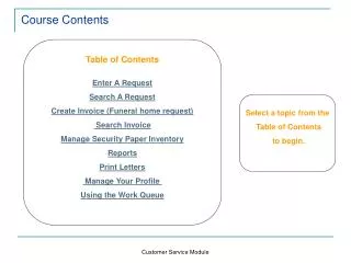
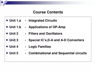
Course Contents • Unit 1.a - Integrated Circuits • Unit 1.b - Applications of OP-Amp • Unit 2 - Filters and Oscillators • Unit 3 - Special IC’s,D-A and A-D Converters • Unit 4 - Logic Families • Unit 5 - Combinational and Sequential circuits
Text Books:1. Linear Integrated Circuits – D. Roy Choudhury2. Op-Amps & Linear ICs – Ramakanth A. Gayakwad.3. Digital Fundamentals – Floyd and Jain
Unit 1- Integrated Circuits • What is an Integrated Circuit? • Where do you use an Integrated Circuit? • Why do you prefer an Integrated Circuit to the circuits made by interconnecting discrete components?
Def: The “Integrated Circuit “ or IC is a miniature, low cost electronic circuit consisting of active and passive components that are irreparably joined together on a single crystal chip of silicon. In 1958 Jack Kilby of Texas Instruments invented first IC
Applications of an Integrated Circuit • Communication • Control • Instrumentation • Computer • Electronics
Advantages: • Small size • Low cost • Less weight • Low supply voltages • Low power consumption • Highly reliable • Matched devices • Fast speed
Integrated circuits Monolithic circuits Bipolar Uni polar Dielectric isolation JFET MOSFET Classification • Digital ICs • Linear ICs Hybrid circuits Thick &Thin film Pn junction isolation Classification of ICs
Chip size and Complexity • Invention of Transistor (Ge) - 1947 • Development of Silicon - 1955-1959 • Silicon Planar Technology - 1959 • First ICs, SSI (3- 30gates/chip) - 1960 • MSI ( 30-300 gates/chip) - 1965-1970 • LSI ( 300-3000 gates/chip) -1970-1975 • VLSI (More than 3k gates/chip) - 1975 • ULSI (more than one million active devices are integrated on single chip)
Factors affecting selection of IC package • Relative cost • Reliability • Weight of the package • Ease of fabrication • Power to be dissipated • Need of external heat sink
Temperature Ranges • Military temperature range : -55o C to +125o C (-55o C to +85o C) • Industrial temperature range : -20o C to +85o C (-40o C to +85o C ) • Commercial temperature range: 0o C to +70o C (0o C to +75o C )
Operational Amplifier The operational amplifier (Op-Amp) is a multi- terminal device which internally is quite complex.
Operational Amplifier An “Operational amplifier” is a direct coupled high-gain amplifier usually consisting of one or more differential amplifiers and usually followed by a level translator and output stage. The operational amplifier is a versatile device that can be used to amplify dc as well as ac input signals and was originally designed for computing such mathematical functions as addition, subtraction, multiplication and integration.
Basic Information of Op-Amp Op-amps have five basic terminals, that is, two input terminals, one output terminal and two power supply terminals.
Packages The metal can (TO) Package The Flat Package The Dual-in-Line (DIP) Package
Basic Information of an Op-amp contd… Power supply connection: The power supply voltage may range from about + 5V to + 22V. The common terminal of the V+and V- sources is connected to a reference point or ground.
Manufacturer’s Designation for Linear ICs • Fairchild - µA, µAF • National Semiconductor - LM,LH,LF,TBA • Motorola - MC,MFC • RCA - CA,CD • Texas Instruments - SN • Signetics - N/S,NE/SE • Burr- Brown - BB
Fairchild’s original µA741 is also manufactured by other manufactures as follows • National Semiconductor - LM741 • Motorola - MC1741 • RCA - CA3741 • Texas Instruments - SN52741 • Signetics - N5741
741 Military grade op-amp • 741C Commercial grade op-amp • 741A Improved version of 741 • 741E Improved version of 741C • 741S Military grade op-amp with higher slew rate • 741SC Commercial grade op-amp with higher slew rate
Differential Amplifier V0 =Ad (V1 – V2 ) Ad =20 log10 (Ad ) in dB Vc = CMRR= ρ = | |
Characteristics and performance parameters of Op-amp • Input offset Voltage • Input offset current • Input bias current • Differential input resistance • Input capacitance • Open loop voltage gain • CMRR • Output voltage swing
Characteristics and performance parameters of Op-amp • Output resistance • Offset adjustment range • Input Voltage range • Power supply rejection ratio • Power consumption • Slew rate • Gain – Bandwidth product • Equivalent input noise voltage and current
Characteristics and performance parameters of Op-amp • Average temperature coefficient of offset parameters • Output offset voltage • Supply current
1. Input Offset Voltage The differential voltage that must be applied between the two input terminals of an op-amp, to make the output voltage zero. It is denoted as Vios For op-amp 741C the input offset voltage is 6mV
2. Input offset current The algebraic difference between the currents flowing into the two input terminals of the op-amp It is denoted as Iios = | Ib1 – Ib2| For op-amp 741C the input offset current is 200nA
3. Input bias current The average value of the two currents flowing into the op-amp input terminals It is expressed mathematically as For 741C the maximum value of Ib is 500nA
4. Differential Input Resistance It is the equivalent resistance measured at either the inverting or non-inverting input terminal with the other input terminal grounded It is denoted as Ri For 741C it is of the order of 2MΩ
5. Input capacitance It is the equivalent capacitance measured at either the inverting or non- inverting input terminal with the other input terminal grounded. It is denoted as Ci For 741C it is of the 1-4 pF
6. Open loop Voltage gain It is the ratio of output voltage to the differential input voltage, when op-amp is in open loop configuration, without any feedback. It is also called as large signal voltage gain It is denoted as AOL AOL=Vo / Vd For 741C it is typically 200,000
7. CMRR It is the ratio of differential voltage gain Ad to common mode voltage gain Ac CMRR = Ad / Ac Ad is open loop voltage gain AOL and Ac = VOC / Vc For op-amp 741C CMRR is 90 dB
8. Output Voltage swing The op-amp output voltage gets saturated at +Vcc and –VEE and it cannot produce output voltage more than +Vcc and –VEE. Practically voltages +Vsat and –Vsat are slightly less than +Vcc and –VEE . For op-amp 741C the saturation voltages are + 13V for supply voltages + 15V
9. Output Resistance It is the equivalent resistance measured between the output terminal of the op-amp and ground It is denoted as Ro For op-amp 741 it is 75Ω
10. Offset voltage adjustment range The range for which input offset voltage can be adjusted using the potentiometer so as to reduce output to zero For op-amp 741C it is + 15mV
11. Input Voltage range It is the range of common mode voltages which can be applied for which op-amp functions properly and given offset specifications apply for the op-amp For + 15V supply voltages, the input voltage range is + 13V
12. Power supply rejection ratio PSRR is defined as the ratio of the change in input offset voltage due to the change in supply voltage producing it, keeping the other power supply voltage constant. It is also called as power supply sensitivity (PSV) PSRR= (Δvios / ΔVcc)|constant VEE PSRR= (Δvios / ΔVEE)|constant Vcc The typical value of PSRR for op-amp 741C is 30µV/V
13. Power Consumption It is the amount of quiescent power to be consumed by op-amp with zero input voltage, for its proper functioning It is denoted as Pc For 741C it is 85mW
14. Slew rate It is defined as the maximum rate of change of output voltage with time. The slew rate is specified in V/µsec Slew rate = S = dVo / dt |max It is specified by the op-amp in unity gain condition. The slew rate is caused due to limited charging rate of the compensation capacitor and current limiting and saturation of the internal stages of op-amp, when a high frequency large amplitude signal is applied.
Slew rate It is given by dVc /dt = I/C For large charging rate, the capacitor should be small or the current should be large. S = Imax / C For 741 IC the charging current is 15 µA and the internal capacitor is 30 pF. S= 0.5V/ µsec
S =slew rate = = Vmωcosωt max Slew rate equation Vs = Vm sinωt Vo = Vm sinωt S = Vm ω = 2 π f Vm For distortion free output, the maximum allowable input frequency fm can be obtained as S = 2 π f Vm V / sec This is also called full power bandwidth of the op-amp
15. Gain – Bandwidth product It is the bandwidth of op-amp when voltage gain is unity (1). It is denoted as GB. The GB is also called unity gain bandwidth (UGB) or closed loop bandwidth It is about 1MHz for op-amp 741C
16. Equivalent Input Noise Voltage and Current The noise is expressed as a power density Thus equivalent noise voltage is expressed as V2/Hz while the equivalent noise current is expressed as A2 /Hz
17. Average temperature coefficient of offset parameters The average rate of change of input offset voltage per unit change in temperature is called average temperature coefficient of input offset voltage or input offset voltage drift It is measured in µV/oC. For 741 C it is 0.5 µV/oC The average rate of change of input offset current per unit change in temperature is called average temperature coefficient of input offset current or input offset current drift It is measured in nA/oC or pA/oC . For 741 C it is 12 pA/oC
18. Output offset voltage ( Voos ) The output offset voltage is the dc voltage present at the output terminals when both the input terminals are grounded. It is denoted as Voos
19. Supply current It is drawn by the op-amp from the power supply For op-amp 741C it is 2.8mA
Factors affecting parameters of Op-amp Supply Voltage Frequency Temperature • Input offset current • Input offset voltage • Input bias current • Power consumption • Gain-Bandwidth product • Slew rate • Input resistance • Voltage gain • Input resistance • Output resistance • CMRR • Input noise voltage • Input noise current • Voltage gain • Output Voltage swing • Input voltage range • Power consumption • Input offset current
Absolute Maximum Ratings of Op-amp • Maximum power dissipation: This is the maximum power which can be dissipated, in the internal stages of the op-amp in the form of heat • Operating temperature range: As specified in the data sheet, op-amp can work satisfactorily, over the operating temperature range, as required for the given application
Absolute Maximum Ratings of Op-amp • Maximum supply voltage: This is the maximum d.c. supply voltage which can be applied to the op-amp • Maximum differential input voltage: This rating gives the maximum value of difference between the two input voltages, applied to the two input terminals of the op-amp
Absolute Maximum Ratings of Op-amp • Maximum common mode input voltage: This is the maximum value of the input voltage which can be simultaneously applied to the two input terminals • Storage temperature range: This gives the temperature range over which the op-amp can be stored safely.