On your Wavelength!
advanced device fabrication. signal. detector. lock-in detector. 16.0. material character-isation. 65. o. filter. device character-isation. 14.0. 60. o. 55. o. 12.0. basic theory. 50. o. spectrometer. 10.0. test structure fabrication. 45. o. 8.0. 40. o. device

On your Wavelength!
E N D
Presentation Transcript
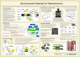
advanced device fabrication signal detector lock-in detector 16.0 material character-isation 65 o filter device character-isation 14.0 60 o 55 o 12.0 basic theory 50 o spectrometer 10.0 test structure fabrication 45 o 8.0 40 o device modelling 35 physical device concept 6.0 o LOAD (120 Ton) 30 Hydrostatic pressure measurements o lamp 4.0 Example: avalanche breakdown in semiconductors 25 o rotatable sample optical fibre 2.0 electrical connections 20 o • different materials are found to exhibit very different pressure dependence of breakdown voltage (Vb) • this demonstrated the role of the bandstructure in determining behaviour at high electric fields • high pressure changes the lattice constant • electronic and vibrational properties change • the role of bandstructure in optoelectronic devices can be conveniently investigated • the effect is similar to a change in composition…. =13 0.0 o reference new device design angle wafer growth upper piston -2.0 pre-stressed double cylinder chopper laser 1.86 1.88 1.90 1.92 1.94 1.96 1.98 2.00 conic, insulated feedthroughs Al foil fibre in epoxy-filled stub device under test pressure-transmitting fluid manganin coil pressure gauge O-ring seal phosphor-bronze ring lower piston • a simple 15kbar piston-cylinder pressure cell allows variation of the bandgap by about 10% • optical and electrical access to the sample • other systems available in ODM include helium gas cells and diamond anvil cells, offering wide pressure range and low temperature operation. optical storage optical telecom imaging radar Applications: sensing wireless displays Experimental tools: tunable lasers / OPA THz beam Free Electron Laser Ultrafast electronics Theoretical calculations Structural, electronic and optical properties of quantum dots • Example: AlGaN/GaN wurtzite quantum dots • form truncated hexagonal pyramids • calculations using Fourier-domain Green’s function method Electron wavefunctions UV visible NIR MIR FIR MMW RF • thin layers of semiconductors grown on substrates with different lattice constant self-organise into small ‘quantum dots’ • these quantum dots have desirable properties for lasers due to their atomic-like electron density of states Spectral range: GaN InGaAs Pb salts Electronics: Si, SiGe GaAs Materials for sources: InGaAsP HgCdTe • Example: micrograph of stacked InAs QDs in a GaAs matrix (courtesy of Paul Koenraad, TU Eindhoven) dilute nitrides: GaInNAs GaInNSb Novel materials/ structures: • Theoretical calculation of QD optical properties must include: • shape of self-organised quantum dot • strain distribution • piezoelectriceffects • electronicproperties inter-subband lasers: Quantum Cascade • Strain and piezoelectric effects cause electron and hole wavefunctions to be non-overlapping for ‘large’ (height>2nm) QDs. • Drastic consequences for light emission! • The size and composition can be designed to maximise the overlap. QW1 QW2 CM (x5) (x3) E E E E 1 2 3 4 Hole wavefunctions Semiconductor Materials • Modulated reflectance spectroscopy • non-contact, non-destructive method • yields information on ground and excited quantum states • new line-fitting procedure identifies multiple levels • Example: mapping electronic and optical resonances in resonant cavity light-emitting diodes • Silicon is ubiquitous in electronics, but interacts relatively weakly with light • direct-gap III-V’s are used for light emission and detection in the visible and near-infrared • GaInAs lattice-matched toInP dominates applications in optical telecoms • III-N materials (AlN, GaN, InN) allow blue-green light emitters • “dilute nitrides” (GaNAs, GaInNAs) are promising for the infrared (large bowing gives small bandgap) • not only the bandgap, but also energies of ‘critical points’ in the bandstructure (EG, EL, EX) are important for optoelectronic device performance AlGaAs distributed Bragg reflector Photoreflectance spectra, identifying energy of quantum well emission lines (QW1, QW2) and cavity mode (CM), as function of angle group GaAs Common tetrahedral (zincblende) semconductors: group IV III-V II-VI AlGaInP optical cavity - controls optical resonance photoreflectance signal (arbitrary units) GaInP H H H H 1 2 3 4 AlGaInP ~50nm GaAs distributed Bragg reflector period AlGaAs Apparatus for modulated reflectance spectroscopy quantum well - light emission at electronic resonance (x3) II III IV V VI Data Schematic of all-semiconductor resonant cavity visible light-emitting diode Fit ~50nm 2 B N C O Al Si P S 3 energy (eV) Zn Ga Ge As Se 4 Visible wave-lengths: displays Cd In Sn Sb Te 5 1.3 µm, 1.55µm telecoms bands Optoelectronic Devices and Materials Group University of Surrey http://www.ph.surrey.ac.uk/odm Semiconductor Materials for Optoelectronics The Optoelectronic Devices and Materials Research Group (ODM) studies the structural, electronic and optical properties of semiconductor materials important for the electronics and communications industries. • On your Wavelength! • Materials which emit, detect, transmit, or switch light at different wavelengths are important for a range of applications. • Near-infrared lasers and detectors are used in optical fibre communications - the hardware underpinning the IT revolution. • Visible (red) lasers are used in consumer electronics for optical storage (CDs, DVDs) • Blue light emitters based on GaN are opening up applications in displays and high-density DVDs • New materials (e.g. dilute nitrides) and new structures (e.g. Quantum Cascade lasers) offer improved light emitters in the mid-infrared, a region of growing importance for chemical sensing (e.g. pollutants), process control, etc. • new TeraHertz sources and detectors in the far-infrared to millimeter wave range are opening up new imaging technologies at the optics-radiowave boundary • Modus Operandi • Experiment and Theory • close collaboration between experimentalists and theorists within ODM • Industrial Collaboration • ODM has research collaborations with many of the major companies in photonics and telecoms • Fundamental physics using advanced real-world devices • extremely pure, precision-grown materials are also excellent for discovering new physics and new device concepts! • Methods • wide range of experimental and theoretical methods for the investigation of structural, electrical and optical properties of semiconductors and opticalmicrostructures • Experimental methods • Theoretical methods • wide range of standard methods: optical, electronic, cryogenic • application of hydrostatic pressure to optoelectronic devices and materials • novel modulated reflectance methods • users of FELIX Free Electron Laser • new Femtosecond Laser laboratory • bandstructures and transition rates of semiconductor nanostructures • mechanical-electronic-optical properties of strained semiconductors • novel ultrafast photon-electron interactions and transport ODM industrial collaborator