Download
1 / 20
250 likes | 573 Vues
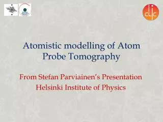
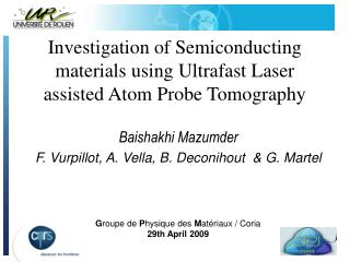
Investigation of Semiconducting materials using Ultrafast Laser assisted Atom Probe Tomography. Baishakhi Mazumder F. Vurpillot, A. Vella, B. Deconihout & G. Martel. G roupe de P hysique des M atériaux / Coria 29th April 2009. Plan. Introduction to Atom Probe Tomography

E N D
Investigation of Semiconducting materials using Ultrafast Laser assisted Atom Probe Tomography Baishakhi Mazumder F. Vurpillot, A. Vella, B. Deconihout & G. Martel Groupe de Physique des Matériaux / Coria 29th April 2009
Plan • Introduction toAtom Probe Tomography • Ultra-short Pulse Laser Assisted Atom Probe • Applications • Silicon Field evaporation • Theoretical interpretation • Conclusion & Perspectives
Position Sensitive Detector (X,Y,TOF) Radius R<100 nm Y X Atom Probe Tomography • APT = FIM + TOF • Tip subjected to field F~V/R and the evaporation • rate follows the Arrhenius law • Tip pulsed field evaporated atom by atom • Ions projected on a PSD • TOF mass spectrometry • 3D reconstruction of the atomic distribution • Volume ~100x100x100 nm3 • Spatial Resolution - 0.2nm in depth • 0.5nm laterally L V
Femtosecond laser assisted atom probe τpulse DSpot Laser beam • Energy used ~ 0.1 – 100 μJ /pulse • Dspot~ 100-800 μm • τpulse ~40-500 fs • on-demand wavelength (infrared-visible-UV) • repetition rate 1-100 kHz Tip B. Gault, et al. Rev. Sci. Instrum. 77, 043705 (2006)
Laser Assisted Tomography Atom Probe R<100nm R Ion tip -10 P < 10 Pa T < 20-80K PSD V < 20 kV 0 Femtosec laser,100kHz 500fs fs laser pulse Green UV 3 Colour box Stop IR signal Start signal Time of flight Specimen Needle Shape
Applications of Different Aspects SiCo CoFeTb multilayer FeMgOFe MgO Fe 100 nm M.Gilbert et al. Ultramicroscopy 107,767,2007 A. Grenier et al. JAP 102,033912 2007 Talaat Al Kassab, IJMR 99,5,2008 Chemical nature of the material mass to charge ratio obtained by TOF measurement Wide range of materials - All metallic materials - Alloys - Multiple quantum well - Nano wires m mass of the ion,V the DC voltage L,flight length,t flight time,k constant
Mechanism for Field evaporation eEx CB vacuum 2 hn hn 3 1 VB Thermal evaporation Ilas is the intensity of laser applied to the tip. The energy deposited by the laser pulses on the specimen increases its temperature allowing the surface atoms to be ionised. Evaporation rate Photo ionisation n, no of photon absorbed to ionise one atom. This process occurred only on semiconductor or oxide surfaces due to the presence of band gap Tsong et al J. Chem. Phys., 65(6) 1976 Tsong, PRB 30(9) 1984
Mass spectra of Silicon under Infra Red Femtosecond Laser at 80K Condition for good mass resolution photon energy(1.2eV) Measured flux is linearly dependent on laser intensity For the first time we have demonstrated that it is a single-photon process. I.e. the rate of evaporation can be written as: Metal Silicon Zone 2 Zone 1 n, number of photon One photon Best Poster Award, IFES 2008 B.Mazumder,A.Vella,M.Gilbert,B.Deconihout,G.Schimtz Submitted to Surface Science Intensity GW/cm2
Mass spectra of Silicon under Infra Red Femtosecond Laser at 80K Condition for good mass resolution Metal Bad mass resolution with higher laser energy Loosing events close to Si mass There is a saturation after a certain laser energy Silicon Zone 2 Zone 1 Intensity (GW/cm2 )
Study of Si mass spectra with different wavelength at 80K Photon energy 1.2 eV (IR) There is a hump appeared with increasing laser energy with photon energy of near band gap energy. Photon energy 2.45eV (Green) Non existence of the hump in mass spectrum by using laser energy with photon energy higher than the band gap energy.
Existence of hump in SiC using photon energy of near band gap energy Existence of hump in SiC using photon energy of near band gap energy (Green) Photon energy - 2.45eV Evidence of hump with photon energy of near band gap energy Photon energy - 3.62eV (UV) No evidence of hump, even by increasing laser energy; and no variation in mass spectra. CONCLUSION The hump seems to appear only using photons with near-band gap energies
Model Y Initial conditions: S(z)- S(z)+ diameter <<1000 nm Absorption ~10 cm-1 dV Z I/I0~1 Homogeneous absorption Localized injected carrier density 2-steps transition Temporal evolution: N2 (z,t), injected electron density with a relaxation time 2 Relaxation time 2 N1 (z,t), thermalised electron density with a relaxation time 1 E2=0.1 eV Total energy given to the lattice 1.2 eV Relaxation time 1 Spatial evolution: E1=1.1 eV Using simple Fourier equation with a generation term and an approximation on time evolution of Cv(T) with:
Results from Simulation Band structure of Si at 300 K Laser intensity Photon energy 1.2 ev, K=100 W/mK, Heated zone 200 nm h=1.2 eV 0.1 eV 1.1 eV
Results from Simulation Laser intensity Band structure of Si at 300 K Photon energy 1.2 ev, K=100 W/mK, Heated zone 200 nm Laser intensity 1.35 eV h=2.45 eV 1.1 eV Photon energy 2.2 ev,K=100 W/mK, Heated zone 200 nm
Conclusion & Perspectives • Ultra-short laser pulses have been utilized to control atom evaporation • We propose a model to explain particular evaporation flux observed with near-resonant band gap excitation • This model can not explain the observed saturation of photon absorption • Perhaps it can be explained by band bending… Work under progress • Are optical nonlinear absorptions an efficient process ?…Work under progress • Are diffusive transport plays a role in the evaporation process ? • Atom probe tomography is sensitive to thermal processes in the fs range when near-resonant band gap illumination is used
THANK YOU FOR YOUR ATTENTION
Sample preparation • Two steps for sample preparation • Lift out method (CAMECA) • Annular milling Deposition of protection cap : Pt Ion deposition (~1µm) Cut a lamella by FIB “Welding” it to the micromanipulator Bringing it in contact with a support pillar Welding it and cutting a portion of tip
Annular Milling The sample is aligned along the beam direction, the inner diameter of the circular mask and the milling current are reduced after each milling stage. 1 m h d Si Rough Mill Sharpening Final 0.5-1nA,30 keV 20-100pA, 30keV few pA, minimum Ga acceleration h > 2 x d
Model Y Initial conditions: S(z)+ S(z)- Z diameter <<1000 nm Absorption ~10 cm-1 dV I/I0~1 Homogeneous absorption Localized injected carrier density 2-steps transition Temporal evolution: N2 (z,t), injected electron density with a relaxation time 2 Relaxation time 2 E2=0.1 eV Total energy given to the lattice 1.2 eV N1 (z,t), thermalized electron density with a relaxation time 1 Relaxation time 1 E1=1.1 eV Spatial evolution: Using simple Fourier equation with a generation term and an approximation on time evolution of Cv(T)