Download
1 / 30
300 likes | 319 Vues
This workshop explores various approaches and possibilities for simulating the ps-Detector electronics, including discriminators, TDCs, and TACs, using advanced simulation tools.

E N D
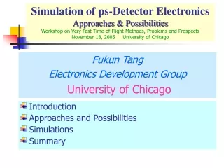
Introduction Approaches and Possibilities Simulations Summary Simulation of ps-Detector ElectronicsApproaches & PossibilitiesWorkshop on Very Fast Time-of-Flight Methods, Problems and ProspectsNovember 18, 2005 University of Chicago Fukun Tang Electronics Development Group University of Chicago
64 master anode pads per tube Signal summed by equal timing traces on a single collector Mismatched terminations INTRODUCTION: Tube Signal Modeling Anode Pad Collector Electronics Board Buried Vias Cross-Section of Anode Board
Tube Output Signal on Collector Signal on the tube collector from Tim’ simulation Rising time 25ps Pulse width (FWHM): 40ps Reflection coefficient: -0.98 (RL=100 ohms) Reflection delay (round trip): 240ps Recovery time: 75ns (Settled at 1ppm) 25ps 240ps 40ps 75ns@1ppm
Ps-Detector Electronics Requirements PMT Output Signal Start 1ns Reference Clock Stop Tw 1ps rms Resolution Time-to-Digital Converter!!!
Approaches and Posibilities • Discriminators • Leading-edge discriminator • Constant fraction discriminator • Different types TDCs • Wilkinson (Mixed) • Time to Amplitude Converter (TAC)(Analog) • “Direct” measurement (Digital) Historical techniques come back but with latest technology!
Approaches & Possibilities From Harold’s talk, we will build two Chips for Tube Readout (1) psFront-end (2) psTransport Time Stamp & Data Buffers “Zero”-walk Disc. 11-bit ADC Data Driver Receiver PMT TAC CK0 11-bit 5Ghz Counter 1:200 Time Stretcher 1Ghz PLL 5Ghz PLL CK1 4x1Ghz PLL Chip1 Chip2
Simulation Tools Spice based Simulators: (1) Cadence: Spectre (analog) (2) Mentor Graphic: Accusim (analog) (3) Cadence: Virtuoso (mixed signal) (4) Mentor Graphic: Eldo, Eldo-RF
Preliminary Simulation Work One Simulation Based on Behavioral Model: SIM-I:“Zero-walk” Discriminator Three Simulations Based on IHP 0.25mm BiCMOS Process: SIM-II:Zero-crossing Comparator SIM-III:1:200 Time Stretcher SIM-IV:Time-to-Amplitude Converter (TAC)
Introduction to IHP 0.25mm BiCMOS SiGe Process • 0.25mm CMOS technology NMOS: Isat=537ma @ WxL=25x0.28mm2 PMOS: Isat=-230ma @ WxL=25x0.28mm2 • 4 metal layers (Al) and one MIM (metal-insulator-metal) layer 1f/mm2 Current densities: M1: 0.85ma/mm M2: 1.00ma/mm M3: 1.00ma/mm M4: 3.40ma/mm Gatepoly: 0.25ma/mm • SiGe based NPN HBT (heterojunction bipolar transistor) SGC25A: ft=60Ghz, Ic=0.5-63ma SGC25B: ft=120Ghz, Ic=0.5-63ma SGC25C: ft=200Ghz, Ic=0.5-63ma • High dielectric stack for RF passive component • CMOS core voltage 2.5V • Why we choose this process? • Very low jitter discriminators • Very low jitter phase locked loops
SIM-I: “Zero-Walk” Discriminator Schematics Tw Constant Fraction Discriminator Start 1ns extra-time delay added Very fast Zero-Crossing voltage Comparator Stop
SIM-I: “Zero-walk” Discriminator Behavioral Model Simulation 10 Input Signals:Tr=15ps, V=7mV to 70mV “0” walk at “0”-Crossing 0 50p 100p 150p 200p 250p Constant fraction attenuator: f=1/3 Delay line: Td=20ps Shapes input signal to a zero-crossing bipolar signal
SIM-I: “Zero-walk” Discriminator Behavioral Model Simulation Results 10x amplitude changes (7mv – 70mV) Reflection Tr=15ps “Walk”=10ps Leading-Edge Disc. Output “walk”=“0”ps Constant Fraction Disc. Output Time Interval Latch Output 0 50p 150p 200p 250p 300p 350p 400p 450p 500p 100p
SIM-II: Zero-Crossing Voltage Comparator Schematics Based on IHP 0.25mm BiCMOS Process 2 gain Stages, 2 level shifters, A =400
SIM-II:Zero-Cross Comparator Preliminary Simulation Results + 1.56V 0.8V 0 25p 50p 75p 100p Comparator Outputs @ Input Signal 1mV to 10 mV Sweep (Increment = 1mV)
SIM-II: Comparator Simulation Results • Simulation input signal 1-10mV square pulses. • Output is fully saturated at 8mV input signal. • Output swing is 1.6V in differential. • Skew time less than 2.5ps at 10 time signal size changes (full width) • More comprehensive simulation needed
SIM-III: Wilkinson Type TDC SimulationBipolar Time Stretcher: Functional Block Ts = Tw + K Tw + p K = Isc – Isk p = pedestal Isc=200i Tw 1ns C Vc Tw Isk=i 200ns Ts CK EN Data CK 5Ghz counter
SIM-III: Bipolar Time Stretcher Schematics based on IHP 0.25mm BiCMOS Process i-source and i-sink use Behavioral models Ratio = 200
SIM-III: Simulation Result of Stretched Time Interval vs. Input Time Interval Stretched time interval output signal Stretched Time = 274ns (pedestal=74ns) 1ps Time Interval Input Signal 0 50ns 100ns 150ns 200ns 250ns 300ns
SIM-III: Charge and Discharge Switches Caused Overshoot and Undershoot on Time Stretcher Output 250mV overshoot Input Time Signal 1ns Stretched output Signal -50mV undershoot 0 2.5ns 5.0ns 7.7ns
SIM-IV: TAC Simulation Start: Vc = K Tw + p Stop: Vc Hold Reset RESET tw2 Tw tw1 Tw C i_sink vc1 vc2 TAC OUT
SIM-IV: Time-to-Amplitude (TAC) Schematics Based on IHP 0.25mm BiCMOS Process Switch Forward Charge Cancellation
SIM-IV: TAC Output vs. Tw = 1ns Input TAC Reset 1ps Time Interval Input 1ns Slop= -640uV/ps TAC Voltage Output Vc Hold for ADC Reset Ready TAC
SIM-IV: TAC Simulation ResultsSweep Tw from 1ns to 2ns with 100ps Increment Tw=1ns Tw=2ns 10 Different Tw Inputs 10 TAC Outputs Vc(1ns) Vc(2ns)
SIM-IV: TAC Outputs vs. Tw Inputs Sweep Tw from 1ns to 1.01ns with 1ps Increment Tw=1000ps Tw=1001ps Tw=1002ps Tw=1003ps Tw=1004ps Tw=1005ps Tw=1006ps Tw=1007ps Tw=1008ps Tw=1009ps TAC Sensitivity = - 640uV/ps
Wilkinson TDC Vs. TAC-ADC Based on IHP 0.25mm BiCMOS SiGe Process
REVIEW OF IC DESIGN TOOLS Design Stage Digital Analog Behavioral Modeling VHDL, Verilog VHDL-AMS, Verilog-AMS Behaviroral Simulation Modelsim Spectre, Accusim, Eldo Synthesis/optization Leonardo --- Test SynthesisSynopsys-DC+ --- Schematic Capture Virtuoso Composer Virtuoso Composer Pre-Layout Simulation/AnalysisUnknown AnalogArtist (Spectre, Eldo) LayoutDesign Planner Virtuoso-XL Silicon Ensemble-PKS Verification Calibre, XCalibre, Assura Calibre, XCalibre, Assura Post-Layout Simulation/AnalysisUnknown AnalogArtist (Spectre, Eldo) Tools are decided by foundries’ “design kit”!
Conclusion • Very challenging! • Both TDCs are very possible to do the job Wilkinson Time Stretcher TDC TAC-ADC type TDC • Lots of comprehensive simulations need to be done to find the direction to move. • Processes play the key role to win!
Forward Charge Injections without Cancellation Switch Ready Reset TAC ADC Reset Forward Charge Injections Reset i_charge Tc C 4mv/box i_discharge
Forward Charge Injection : Vc(error)=(Cd/C+Cbc)Vd (Pulse Divider!) I-src Cd Vd C Tw i-sink