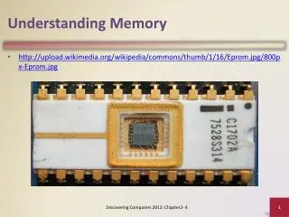
Understanding GPU Memory
Understanding GPU Memory. Instructor Notes. This lecture begins with an example of how a wide-memory bus is utilized in GPUs The impact of memory coalescing and memory bank conflicts are also described along with examples on current hardware

Understanding GPU Memory
E N D
Presentation Transcript
Instructor Notes • This lecture begins with an example of how a wide-memory bus is utilized in GPUs • The impact of memory coalescing and memory bank conflicts are also described along with examples on current hardware • This lecture is important because achieving high memory bandwidth is often the most important requirement for many GPU applications
Topics • Introduction to GPU bus addressing • Coalescing memory accesses • Introduction to memory banks • Memory bank conflicts
Example • Array X is a pointer to an array of integers (4-bytes each) located at address 0x00001232 • A thread wants to access the data at X[0] inttmp = X[0]; 0x00001232 0 0x00001236 1 2 X 0x00001232 3 . . . 4 5 6 0x00001248 7 . . . .
Bus Addressing • Assume that the memory bus is 32-bytes (256-bits) wide • This is the width on a Radeon 5870 GPU • The byte-addressable bus must make accesses that are aligned to the bus width, so the bottom 5 bits are masked off • Any access in the range 0x00001220 to 0x0000123F will produce the address 0x00001220
Bus Addressing • All data in the range 0x00001220 to 0x0000123F is returned on the bus • In this case, 4 bytes are useful and 28 bytes are wasted Memory Controller Send an address Receive data Desired element ? ? ? 0 1 2 3 4 0x00001220 0x00001220
Coalescing Memory Accesses • To fully utilize the bus, GPUs combine the accesses of multiple threads into fewer requests when possible • Consider the following OpenCL kernel code: • Assuming that array X is the same array from the example, the first 16 threads will access addresses 0x00001232 through 0x00001272 • If each request was sent out individually, there would be 16 accesses total, with 64 useful bytes of data and 448 wasted bytes • Notice that each access in the same 32-byte range would return exactly the same data inttmp = X[get_global_id(0)];
Coalescing Memory Accesses • When GPU threads access data in the same 32-byte range, multiple accesses are combined so that each range is only accessed once • Combining accesses is called coalescing • For this example, only 3 accesses are required • If the start of the array was 256-bit aligned, only two accesses would be required ? ? ? 0 1 2 3 4 0x00001220 5 6 7 8 9 10 11 12 0x00001240 13 14 15 ? ? ? ? ? 0x00001260
Coalescing Memory Accesses • Recall that for AMD hardware, 64 threads are part of a wavefront and must execute the same instruction in a SIMD manner • For the AMD 5870 GPU, memory accesses of 16 consecutive threads are evaluated together and can be coalesced to fully utilize the bus • This unit is called a quarter-wavefront and is the important hardware scheduling unit for memory accesses
Coalescing Memory Accesses • Global memory performance for a simple data copying kernel of entirely coalesced and entirely non-coalesced accesses on an ATI Radeon 5870
Coalescing Memory Accesses • Global memory performance for a simple data copying kernel of entirely coalesced and entirely non-coalesced accesses on an NVIDIA GTX 285
Memory Banks • Memory is made up of banks • Memory banks are the hardware units that actually store data • The memory banks targeted by a memory access depend on the address of the data to be read/written • Note that on current GPUs, there are more memory banks than can be addressed at once by the global memory bus, so it is possible for different accesses to target different banks • Bank response time, not access requests, is the bottleneck • Successive data are stored in successive banks (strides of 32-bit words on GPUs) so that a group of threads accessing successive elements will produce no bank conflicts
Bank Conflicts – Local Memory • Bank conflicts have the largest negative effect on local memory operations • Local memory does not require that accesses are to sequentially increasing elements • Accesses from successive threads should target different memory banks • Threads accessing sequentially increasing data will fall into this category
Bank Conflicts – Local Memory • On AMD, a wavefront that generates bank conflicts stalls until all local memory operations complete • The hardware does not hide the stall by switching to another wavefront • The following examples show local memory access patterns and whether conflicts are generated • For readability, only 8 memory banks are shown
Bank Conflicts – Local Memory • If there are no bank conflicts, each bank can return an element without any delays • Both of the following patterns will complete without stalls on current GPU hardware 0 0 0 0 1 1 1 1 2 2 2 2 3 3 3 3 4 4 4 4 5 5 5 5 6 6 6 6 7 7 7 7 Thread Memory Bank Thread Memory Bank
Bank Conflicts – Local Memory • If multiple accesses occur to the same bank, then the bank with the most conflicts will determine the latency • The following pattern will take 3 times the access latency to complete Conflicts 0 0 1 1 2 1 2 2 3 3 3 4 4 5 5 1 6 6 1 7 7 Thread Memory Bank
Bank Conflicts – Local Memory • If all accesses are to the same address, then the bank can perform a broadcast and no delay is incurred • The following will only take one access to complete assuming the same data element is accessed 0 0 1 1 2 2 3 3 4 4 5 5 6 6 7 7 Thread Memory Bank
Bank Conflicts – Global Memory • Bank conflicts in global memory rely on the same principles, however the global memory bus makes the impact of conflicts more subtle • Since accessing data in global memory requires that an entire bus-line be read, bank conflicts within a work-group have a similar effect as non-coalesced accesses • If threads reading from global memory had a bank conflict then by definition it manifest as a non-coalesced access • Not all non-coalesced accesses are bank conflicts, however • The ideal case for global memory is when different work-groups read from different banks • In reality, this is a very low-level optimization and should not be prioritized when first writing a program
Summary • GPU memory is different than CPU memory • The goal is high throughput instead of low-latency • Memory access patterns have a huge impact on bus utilization • Low utilization means low performance • Having coalesced memory accesses and avoiding bank conflicts are required for high performance code • Specific hardware information (such as bus width, number of memory banks, and number of threads that coalesce memory requests) is GPU-specific and can be found in vendor documentation

