PS.1TFB Cavity Voltage Feedback & Processing Circuits Guide
170 likes | 271 Vues
This guide provides detailed specifications and diagrams of the PS.1TFB system's cavity voltage feedback and processing circuits. Learn about the Notch Filter, Automatic Delay Unit, and Single Clock Signal Processing. Explore how these components work together to optimize system performance and ensure accurate feedback control. Discover the intricacies of loop delays, harmonic compensation, and cavity group delay to fine-tune your system for optimal operation. Gain insights into notch filter functionality, RF signal processing techniques, and clock signal processing methods. Enhance your understanding of feedback mechanisms and circuitry with this comprehensive guide.

PS.1TFB Cavity Voltage Feedback & Processing Circuits Guide
E N D
Presentation Transcript
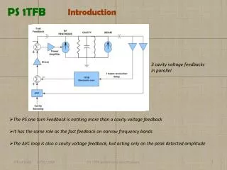
PS 1TFB Introduction 3 cavity voltage feedbacks in parallel • The PS one turn Feedback is nothing more than a cavity voltage feedback • It has the same role as the fast feedback on narrow frequency bands • The AVC loop is also a cavity voltage feedback, but acting only on the peak detected amplitude PS 1TFB preliminary specifications
PS 1TFB Block diagram of the present circuit • The Notch filter removes the contribution from the rf signal to avoid affecting the AVC loop. This unit can be disabled when the AVC loop is disabled (Voltage program = 0) • The Comb filter enhances the revolution lines where the beam signal is located • The automatic delay, together with the clock generation circuit, makes such that the loop delay adapts to the revolution time and harmonic value changes. PS 1TFB preliminary specifications
PS 1TFB Present Automatic Delay unit • The automatic delay, takes care of 4 ingredients of the loop delay • Loop delay in terms of clock periods of the “80 Frev clock”. The sum of the clock delay in the FIFO + clock delay in the remaining circuit needs to be set to the required value at reset. This part of the delay remains equal to the same proportion of the loop delay. • Loop delay in terms of “pure delay” . As this delay doesn’t shrink with the decreasing revolution period, it needs to be compensated for. This is done automatically by inserting the same fixed delay value before the input write clock of the FIFO. • Loop delay in terms of “4 Frf clock”. This delay variation depending on the value of hRF is compensated by a dephasing of the input clock to the FIFO, being a function of the hRF value. • Cavity group delay compensation. This delay needs to be approximated by an harmonic (fixed value=1 presently) of the rf signal. This compensation is dealt with also by a dephasing of the input clock to the FIFO. PS 1TFB preliminary specifications
PS 1TFB Cavity group delay • The cavity frequency response is the one of a 4th order resonator with 2 pairs of poles. • This behavior is due to the use of a tunable resonator in the grid circuit of the final tetrode. • The response of this cavity leads to a +/- 180o phase error at the extreme parts of its bandwidth. This phase error is not compatible with a high gain feedback. • Within its bandwidth, the cavity phase response can be approximated as a fixed group delay ( 300ns). This value remains almost constant over the entire frequency range (to be checked!) • The slope of the cavity phase response can be compensated for as long as the absolute phase at the rf frequency (centre of the system bandwidth) remains equal to zero [modulo 2]. This condition is fulfilled when the total loop delay is a multiple of the rf period. This is the case when the loop delay = TREV – k.TRF = h.TRF – k.TRF . • The best compensation is achieved for the k.TRF closest to the cavity average group delay within its bandwidth. This compensation is adequate even during harmonic changes of the cavity. PS 1TFB preliminary specifications
PS 1TFB Notch Filter • The notch filter is used to make the 1TFB system transparent to the AVC loop. • The AVC loop uses a synchronous low-pass filtered peak detection of the cavity return signal. • This AVC detector is aimed at measuring the RF signal only, although the harmonics of the beam within the bandwidth of the cavity influence the result to some extend. • When the 1TFB is OFF (its feedback signal is disabled before the AVC drive chain summing unit), its presence is not detectable. • When the 1TFB is ON, the loop gain at the rf frequency is high due to the amplification by the comb filter. This effect can be canceled by the insertion of a notch at the rf frequency. • This notch can only be by-passed when the voltage demand is zero (AVC loop off). • Major down-sides of the Notch Filter: • The actual Notch Filter uses a different clock than the remaining part of the circuit. • It necessitates a special treatment in terms of delay • It requires an intermediate analogue conversion. • At a low harmonic value, its delay is a showstopper PS 1TFB preliminary specifications
PS 1TFB Single clock signal processing (1) • The baseband signal processing is well suited as long as the system bandwidth (typ. 3 MHz) is well below the value of the rf frequency. In the actual context, the requirements might be tough for the low-pass filter when using h=7 for instance (fRF = 3.15 MHz). The requirement for a high order filter is not compatible with the loop delay constraint. PS 1TFB preliminary specifications
PS 1TFB Single clock signal processing (2) • Here a partial baseband process selects the rf signal apart from the other revolution harmonics. With a classical LP filter, the limitation would come from its group delay required to remove more than 20 dB at 450 kHz of the parasitic harmonics of the revolution. This big delay can be avoided by using a CIC filter. This approach becomes then acceptable. PS 1TFB preliminary specifications
PS 1TFB Single clock signal processing (3) • As the voltage program is at zero when the cavity harmonic is swept, there is no need to have the notch swept as well. • A Notch could be created with a variable pipeline delay = kD .TCK , with Tck = TREV/hCLK. • The problem is to find an hCLK and kD that fulfill the following equation for all hRF values used in operation. • The delay in the Notch = TRF = TREV/hRF = kD .TCK = kD . TREV/hCLK • hRF = kD/hCKwith hRFЄ [7 , 21] & hCK <160 • The Clock harmonic should thus be the lowest common multiple of all possible rf harmonics. This value is above the 160 set as a limit. PS 1TFB preliminary specifications
PS 1TFB Single clock signal processing (4) • As explained, The Notch Filter was designed to make the 1TFB transparent to the AVC loop. • The 1TFB effect is to lower the gain of the AVC loop by a factor 1/{1+G1TFB(fRF)} • Creating the Above circuit requires that the following constraints are fulfilled: • Dynamic range of the ADC-DAC compatible with the expected value on the Cavities • Added delay in the AVC loop compatible with its stability margin (very likely !) PS 1TFB preliminary specifications
PS 1TFB Single clock signal processing (4) The designed card could just as well manage the AVC loop!! PS 1TFB preliminary specifications
PS 1TFB Improving the present behavior (1) • The circuit presented on the previous slide is likely to offer practical advantages in terms of • Ease of settings-up • Improved stability margin as it can better compensate the Cavity group delay by a change of the k factor in the expression ΔTLOOP = - k.TRF cavity average group delay . • This might be enough to get rid of the faults marginally encountered on the system leading to a cavity power dropout. • Nevertheless, a major sensitivity of the system needs to be highlighted: • Transient beam Loading PS 1TFB preliminary specifications
PS 1TFB Improving the present behavior (2) The present tuning loop makes such that the angle L is kept to zero by comparing the cavity voltage to the grid voltage. The aim is that the tetrode drives a real charge. L is also the quality factor of the 1TFB. Its should stay to zero. In the presence of a beam current, the price to pay is that the bare cavity detuning Z can be far from zero. In the case of a single beam transient, Z will go from a zero value adapted to the no-beam situation to a value adapted to the full beam value. During the transient of the tuner loop, the cavity will be out of phase, implying more drive from the power, less stability in the fast feedback loop, beam loading stability issues (phase-to-amplitude coupling) and a out-of-phase condition from the 1TFB system. The later has often been the little too-much in the PS 10 MHz system. Solution: during this transient, the 1TFB should stay OFF. PS 1TFB preliminary specifications
PS 1TFB Improving the present behavior (3) • In the case of a periodic beam transient, when the ring is just partially filled and that the cavity fill-up time (with fast feedback) is much smaller than the revolution, Z will take an average value such that the average value of L is zero (Tuner loop BW in the order of a couple of kHz). • Indeed, the cavity will never be properly tuned. Its phase error, from the 1TFB point of view will go from a +x error in the presence of beam to a –y error in the absence of beam. • Solution: • a feed-forward acting on the tuning would solve the problem if the bandwidth of the system allowed it (we are far from it!) • A phase compensation value could be deduced from the knowledge of hRF, the number of bunches and the location of the bunches. The (bunch value/average bunch value) would then become the determining factor to deduce the correcting angle to the 1TFB. • N.B.: The real time detuning value could also be used to set the grid tuner for better stability. Although it doesn’t solve the tetrode current requirement problem nor the beam loading stability issue. PS 1TFB preliminary specifications
PS 1TFB Automatic delay The automatic delay could use the architecture of the circuit used in the PS TFB. On top of it should be added the circuit for the cavity delay compensation (the delay of h can either be measured or obtained from a function generator). PS 1TFB preliminary specifications
PS 1TFB Setting-up and maintenance • With the presented architecture, the 1TFB system will much simple to maintain and to set-up • There will be no “blind” potentiometer to set for the gain and offset of the dephasing circuit (used to compensate for the Notch and Cavity delays). Presently these settings are made by creating different fREV and fRF set points and measure the closed loop response. These setting-up is stressful as the power equipment is vulnerable. • There will be no cable to remove or add depending on a change of the actual fixed delay in the loop, nor strap to swap on a PCB in case it requires a change in the FIFO depth at reset . The good value of the delay is determined by the quality of the loop response when changing the revolution frequency. • The system will require no reset at a specific revolution frequency. • An included BTF block would ease the setting-up, by eliminating the need for the cabling of external instruments. An rf output should be made available to feed the Tuner loop. • During the run, the instabilities can be spotted because the signals are deterministic knowing the beam current. The observation of a single REV line on both sides of the rf should inform us. In case of an overrun, the 1TFB loop may be opened and an alarm signal could be sent. • The system will work at least with 14 bits instead of 10 for the Notch and even 8 for the comb filter. PS 1TFB preliminary specifications
PS 1TFB Construction • The absence of a Notch filter together with the double clock speed will allow lengthening the cables and thus will allow to group all the 1TFB boards, belonging to cavities attached to the same tuner circuit, into a single crate. • The PS complex is targeted (although no firm decision has been taken) to work with VME systems of the kind used for the LEIR low-level. The VME 64X / 9U, 160mm-depth, crate would thus be a valuable choice. • The circuit would look like many constructed ADC-FPGA-DAC circuits, but would require the presence of a fine programmable delay like the one used for the LHC 1TFB. This LHC board is a VME 64 / 9U 220mm-depth, not compatible with the VME 64X. This presents the LHC VME crate as a good candidate too! PS 1TFB preliminary specifications
PS 1TFB Conclusion • Suppress the Notch • Create an Adaptative Cavity group delay compensation • Use the PS TFB automatic delay structure with an addition concerning the cavity group delay compensation • Install the AVC loop within the board • Keep the 1TFB loop OFF during transients of the Tuner loop • Create a real time phase compensation circuit for repetitive beam transients. Check if such an improvement could be implemented on the grid resonator of the tetrode. • Install an Instability detector • Install an Inner BTF • VME 64X / 9U, 160mm-depth or LHC RF VME 64 ? PS 1TFB preliminary specifications