Download
1 / 1
10 likes | 172 Vues
is deposited at a number of positions along the line indicated, and the total charge collected by the four pixel diodes is simulated. Laser Test Results

E N D
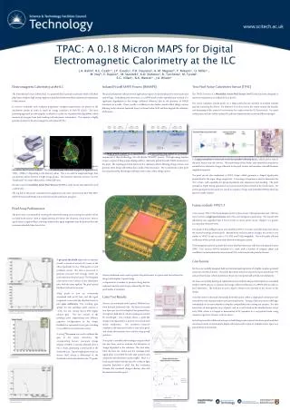
is deposited at a number of positions along the line indicated, and the total charge collected by the four pixel diodes is simulated. Laser Test Results Sensors are stimulated with a pulsed 1064nm laser from the back (substrate) side. The laser is focussed to a 2µm spot size at the depth of the epitaxial layer through the bulk silicon, which is transparent at this IR wavelength. This method allows a point-like charge to be deposited in a pixel to cross-check with device simulations. The correlation between simulation and measured results is seen to be good, and clearly demonstrates how well the deep p-well performs. A test pixel is available with analogue outputs which has also been used to evaluate the behaviour of charge deposited in the substrate. The time delay from the laser fire strobe and the analogue pixel signal pulse is recorded for each laser position, and compared with simulation results (right). There is a fixed system delay from the laser fire strobe to light emission (included in plot), but the correlation between the simulated charge-collection time and the measured result is good. TPAC: A 0.18 Micron MAPS for Digital Electromagnetic Calorimetry at the ILC J.A. Ballinb, R.E. Coathc*, J.P. Crooksc, P.D. Daunceyb, A.-M. Magnanb, Y. Mikamia , O. Millera , M. Noyb, V. Rajovica , M. Stanitzkic, K.D. Stefanovc, R. Turchettac, M. Tyndelc, E.G. Villanic, N.K. Watsona , J.A. Wilsona Charge collection in a non-deep p-well process Charge collection in a deep p-well process preShape pixel circuit block diagram (left) and layout up to first metal layer (right): Dotted line shows the 50µm pixel boundary Illustration showing a SiW ECAL structure in an ILC barrel concept Simulation of a 3-jet hadronic event in an ILC detector A per-pixel threshold scan with no stimulus reveals a spread of around 20 counts in the offset (pedestal) for the 7056 pixels of each preShape variant. This data is processed to generate per-pixel trim settings, which are pre-loaded into the pixel array. The histogram of per-pixel scans is shown in the subsequent plot, with the trims applied: The pixel spread had been reduced to 4 counts. Many pixels in turn are consistently stimulated with an IR laser, and the signal magnitude is recorded (by threshold scan) to plot gain uniformity. The resulting gain spread for two preShape pixel variants is ~12%, but one variant shows 40% higher relative gain. The two variants of the preShape pixel implemented two different capacitor configurations in the shaper feedback for optimised circuit gain according to two different circuit simulator tools. A strong 55Fesource was used to calibrate the gain of the sensor electronics. The corresponding known maximum charge deposit of 1640e- is entirely collected when it hits a diode, generating a small peak in the threshold scan. Typical single-pixel results are shown (left) where a differential of the threshold scan clearly identifies the 55Fe peak. Device simulations were used to predict the performance of a pixel with and without the deep p-well implant. A point charge Histograms of the mean value of per pixel noise without trim settings (above) and with in-pixel trim settings applied (below) Pixel layout layers: n-well (pink), deep p-well (shaded). Profile for simulation & measurement results (below) marked with dotted line. Measurement and simulation results for charge deposited at equivalent points in a pixel preShape pixel gain uniformity in main array: two pixel variants are shown, quad0 (solid) and quad1 (dashed). Single pixel result obtained with a 55Fe source: Regular threshold scan is differentiated to clearly show the 55Fe peak. • Simulation and measured charge collection time for hits occurring between two pixel diodes. • Simulation profiles B & C are close to pixel diodes • Measurement profile passes directly through diodes