Download
1 / 49
560 likes | 849 Vues
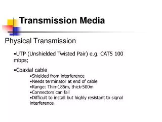
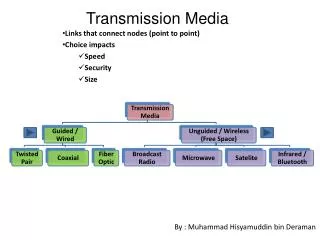
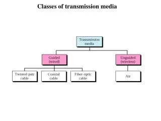
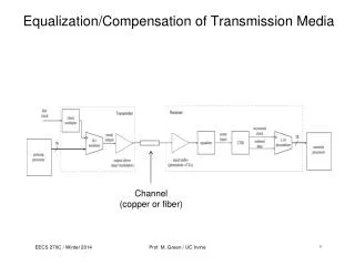
Equalization/Compensation of Transmission Media. Channel (copper or fiber). 1. Optical Receiver Block Diagram. O E. TIA. LA. EQ. CDR. DMUX. ≈ -18 dBm. ≈ 10 µA. ≈ 10 mV p-p. ≈ 400 mV p-p. 2. 4-foot cable. 15-foot cable. Copper Cable Model. Copper Cable.

E N D
Equalization/Compensation of Transmission Media Channel (copper or fiber) Prof. M. Green / UC Irvine 1
Optical Receiver Block Diagram O E TIA LA EQ CDR DMUX ≈ -18 dBm ≈ 10 µA ≈ 10 mV p-p ≈ 400 mV p-p Prof. M. Green / UC Irvine 2
4-foot cable 15-foot cable Copper Cable Model Copper Cable Where: L is the cable length a is a cable-dependent characteristic Prof. M. Green / UC Irvine 2
Effect of Copper on Broadband Data waveform eye diagram Prof. M. Green / UC Irvine 3
Adaptive Analog Equalizer for Copper • Implemented in Jazz Semiconductor SiGe BiCMOS process: • 120 GHz fT npn • 0.35 µm CMOS Prof. M. Green / UC Irvine 4
Equalizer Block Diagram Prof. M. Green / UC Irvine 5
Analog Equalizer Concept (1) Simple linear circuit (normalized to 1Hz): 1 V2 V3 V1 +0.5 -0.5 1 1 1 1 C1 1s simple channel model bandpass filter combined flat response + peaked response Prof. M. Green / UC Irvine 6
1 V2 V3 V1 +0.5 -0.5 1 1 1 1 C1 1s V1 Analog Equalizer Concept (2) V2 Prof. M. Green / UC Irvine 7
Rise time = voltage swing/slew rate Rise time nearly constant over different channels! Analog Equalizer Concept (3) Equalized output pulses: V3 Prof. M. Green / UC Irvine 8
Feedforward Path Vout Prof. M. Green / UC Irvine 9
Equalizer Frequency Response Vcontrol f (Hz) Prof. M. Green / UC Irvine 10
VFFE 0.3 teq= 45ps PW = 108ps teq= 60ps PW = 100ps 0 teq= 75ps PW = 86ps -0.3 2.4 2.5 2.6 2.7 2.8 t (ns) ISI & Transition Time • Simulations indicate that ISI correlates strongly with FFE transition time teq. • Optimum teq is observed to be 60 ps. • Nonlinearities affect pulse shape, but not location of zero crossings. Prof. M. Green / UC Irvine 11
Slicer Restores full logic levels Exhibits controlled transition time Prof. M. Green / UC Irvine 12
Feedback Path Prof. M. Green / UC Irvine 13
V+ V- VS ISS CSS (b) (a) (b) (a) t Transition Time Detector DC characteristic: Transient Characteristic: Rectification & filtering done in a single stage. Prof. M. Green / UC Irvine 14
Integrator Prof. M. Green / UC Irvine 15
Detector + Integrator FFE transition Time tFFE From Slicer tslicer= 60ps From FFE tFFE Vcontrol (mV) 90ps 60 slope detector slope detector 40 75ps 20 60ps 0 -20 45ps -40 15ps -60 0 10 20 30 40 50 _ + t (ns) Vcontrol Prof. M. Green / UC Irvine 16
System Analysis integrator feedforward equalizer Vcontrol tslicer teq detector + Kd H(s) Keq _ detector Kd Keq = 1.5 ps/mV Kd = 2.5 mV/ps int = 75ns Prof. M. Green / UC Irvine 17
Measurement Setup EQ inputs Die under test EQ outputs 231 PRBS signal applied to cable Prof. M. Green / UC Irvine 18
Measured Eye Diagrams EQ output EQ input 4-foot RU256 cable (-5 dB atten. @ 5 GHz) 4.0 ps rms jitter 15-foot RU256 cable (-15 dB atten. @ 5 GHz) 3.9 ps rms jitter Prof. M. Green / UC Irvine 19
Summary of MeasuredPerformance Presented at ISSCC Feb. 2004 Prof. M. Green / UC Irvine 20
Equalization vs. Compensation Equalization is accomplished by inverting the transfer function of the channel. Compensation is accomplished only by canceling the ISI at each unit interval. Electronic Dispersion Compensation (EDC) refers to the electronics that accomplishes compensation of copper or optical transmission media. EDC is becoming especially critical as bit rates increase on legacy equipment (e.g., backplane, optical connectors, optical fiber). Prof. M. Green / UC Irvine 21
Pre-Cursor/Post-Cursor ISI Input pulse (no ISI): T cursor pre-cursor ISI post-cursor ISI 0 T 0 Output pulse: Prof. M. Green / UC Irvine 22
Feedforward Equalization (FFE) Idea: To cancel ISI, subtract a weighted & delayed version of the pulse: output pulse delayed by T: d-1 d0 output pulse: Result with 0 pre-cursor ISI: Prof. M. Green / UC Irvine 23
Feedforward Equalization (2) T Time domain: a1 _ + Frequency domain: Prof. M. Green / UC Irvine 24
Feedforward Equalization (3) N-tap FFE structure: T T T a0 a1 a2 an FFE can cancel both pre- and post-cursor distortion. Prof. M. Green / UC Irvine 25
Feedforward Equalization (4) R R _ Vout + V0 V1 V2 ISS 3-tap summing circuit: negative coefficient Coefficients set by gm of each differential pair. Prof. M. Green / UC Irvine 26
Feedforward Equalization (5) Fractional spacing: 1-tap T-spaced FFE frequency response 5-tap T-spaced FFE eye diagram 1-tap T/2-spaced FFE frequency response 5-tap T/2-spaced FFE eye diagram Prof. M. Green / UC Irvine 27
Adaptation (1) a2 a1 optimum setting Assume original sequenceDin(k) is known. Define error signal e(k) as: ^ ^ where Dout(k) is an appropriately delayed version of Din(k). Steepest Descent Algorithm: step size • Algorithm moves coefficients in direction of decreasing mean-square error. • Step size µ should be made sufficiently small to guarantee convergence. • Requires knowledge of properties of mean-square error; usually not available. Prof. M. Green / UC Irvine 28
Adaptation (2) ^ ^ Least mean-square (LMS) algorithm: FFE output signal: Analog version of LMS: both signals are available on chip. Prof. M. Green / UC Irvine 29
Adaptation (3) Types of adaptation: 1. Training Sequence A training sequence with known properties is sent through the channel + equalizer. The equalizer output is compared to the original sequence and an error signal is generated. 2. Blind Adapation Adaptation is continually performed while system is running. Only limited properties of the signal are known. An error signal must somehow be generated without having the original sequence. Prof. M. Green / UC Irvine 30
Adaptation (4) ^ FFE _ + Generation of error signal: • Slicer restores logic levels and opens eye vertically. • Bit sequences at slicer input & input are identical. • Slicer has no effect on placement of zero crossing. • Slicer can be realized using CML buffers with sufficient gain and speed. Prof. M. Green / UC Irvine 31
Decision Feedback Equalization (DFE) T T T a0 a1 a2 an + - - - bm b2 b1 T T T FFE structure: Noise applied to FFE input will be retained (perhaps filtered) at the output. DFE structure: Prof. M. Green / UC Irvine 32
Decision Feedback Equalization (2) - + - - bm b2 b1 T T T • Slicer is embedded in the structure; Dout is a digital signal. • Delay elements are digital -- commonly realized by DFFs. • Use of slicer suppresses input noise. • Cancels post-cursor distortion only. Prof. M. Green / UC Irvine 33
Decision Feedback Equalization (3) - + - - consistent with bm b2 b1 T T T post-cursor distortion 1-tap example: 2/3 1/3 1 (desired) 1 • Tap weights provide a “look-up table,” canceling post-cursor distortion based on last m bits of output sequence. • DFE can sometimes “latch up” with wrong tap weights during adaptation. 2/3 Prof. M. Green / UC Irvine 34
FFE + DFE T T T a0 a1 a2 an + - - - bm b2 b1 T T T Combined FFE and DFE can be used to cancel both pre- and post-cursor distortion with low noise. Prof. M. Green / UC Irvine 35
Front-End Circuits for DSP-Based Receivers from channel ADC requires strict control over its input amplitude VA. Vin Dout [1:n] VA PGA ADC VC Automatic Gain Control AGC Programmable Gain Amplifier (PGA): where “Linear in dB” gain characteristic gives settling time independent of input amplitude. Prof. M. Green / UC Irvine 36
PGA Design 1. Differential Pair: 2. Source Degeneration: 3. Op-Amp with Feedback: Rf Iout- Iout+ Iout- Iout+ RS Vin+ Vin- Vin+ Vin- + + Vin Vout RS _ _ 2RS ISS Rf + VC _ For biasing in weak inversion: RS varied with constant dB per step. Prof. M. Green / UC Irvine 37
PGA Example (1) C.-C. Hsu, J.-T. Wu, “A highly linear 125-MHz CMOS switched-resistor programmable-gain amplifier,” JSSC, Oct. 2003, pp. 1663-1670. Realization of RS: 2 dB steps Prof. M. Green / UC Irvine 38
PGA Example (2) J. Cao, et al., “A 500mW digitally calibrated AFE in 65nm CMOS for 10Gb/s links over backplane and multimode fiber,” ISSC 2009, pp. 370-371. gain of single diff. pair where N = number of diff. pairs turned on Prof. M. Green / UC Irvine 39
Track & Hold Circuit The T/H circuit is comprised of two switch-capacitor stages and an amplifier which provides gain and isolation. Dummy switches are used to cancel channel charge injection and achieve better linearity. 40
Simulation Results T/H differential output for fin = 1.5 GHz and fs=10 GS/sec 41
High-speed Comparator High-Level Clocking: • Improves isolation between the input and output, reducing kickback from output. • Cascoding of the clock switches reduces the Miller effect of the input transistors. • Reduced headroom 42
Metastable Behavior (1) Comp./Latch output T/H output What is the probability of this error occurring? Metastable event 44
Metastable Behavior (2) R R Ct Ct + + v1 v2 − − 45 t
Metastable Behavior (3) Vout (digital) 11 10 01 00 Vin (analog) 2e 0 1 2 3 2Vdec +e -e VLSB -Vdec +Vdec Vdec = minimum detectable logic level e = minimum input at t = 0 so that output level is ≥ Vdecat t = T/2 Including comparator gain: Error probability: 46
Metastable Behavior (4) Recall: For error-free operation after half-clock period: t Error probability: 47
Latch output Reducing Metastability Errors Additional high-speed latches following the comparator/latch stage reduces probability of metastable events at the output. 48