Download
1 / 52
540 likes | 769 Vues
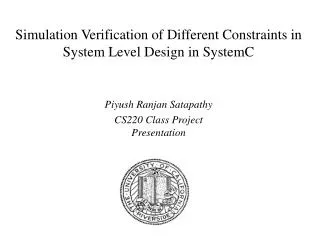
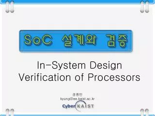
In-System Design Verification of Processors. Macro Instruction Level Simulator (Behavioral) General Purpose Register, Memory Micro-code Level Verifier + Internal Bus Verilog Hardware Model + Clock-cycle Accurate Description. ISS. ADD. SUB. end. Cycle-based. macroSUB. Verilog (HDL).

E N D
Macro Instruction Level Simulator (Behavioral) General Purpose Register, Memory Micro-code Level Verifier + Internal Bus Verilog Hardware Model + Clock-cycle Accurate Description ISS ADD SUB end Cycle-based macroSUB Verilog (HDL) Introduction • Design Hierarchy
What is ISV? • ISV = In-System Verification • When is ISV required? • 1) Design refinement down along the design hierarchy • Comparison between design levels C1: ISS (Instruction Set Simulator) C2: Cycle-based Model C3: RTL Model specification specification C1 C2 vs. C3 Cn Cn
chip system What is ISV? (cont’d) 2) In-system operation : confirm correct behavior in system environment HW (FPGA) chip I/F HW (slowed) (a) simulation (c) emulation SW SW SW HW (b) all-software (d) Virtual Chip
Simulation • Consistency check between models of different abstraction levels • Instruction Set Simulator (behavioral) • RTL model (structural) • Test Vector • Test Pattern • Random Pattern • Test Program • Application Program SW Stimulus at the I/F
Advantage Disadvantage High efficiency = # of bugs detected size of test vector Confined to the designer’s understanding Test pattern Covers rare cases automatic generation Random pattern Coverage not reliable Available good compromise between coverage & efficiency as benchmark Requires many programs to obtain sufficient coverage Test program Simulates real situations High coverage Application program Excessive verification Low efficiency Various Levels of Design Verification(Test Vectors in Simulation)
All-Software Approach • Modeling System Part in Software • Test Vector • System Software (BIOS, OS) • Application Programs • compatible processor design • Helps detect bugs • When the situation is difficult to reproduce with random patterns (i.e., Instruction’s sensible behavior requires some pre-setting) • When instruction behavior is complex, i.e., CISC instruction • Modeling system parts is difficult when • no source code for the application programs is available SW (chip) SW (system)
HW in FPGA Slowed-down System Time Speed up factor 1 second 107 Actual Hardware 10 seconds 106 Logic Emulation 2 minutes 105 16 minutes 104 3 hours 103 Verification Gap 1 day 102 12 days 101 3 months 1 Software Simulation Emulation • Mapping Gate-level Model in FPGA-based System • Fast ISV • in simulation speed • in design stage
Concurrent Verification Sequential Verification Without Emulation System SW Design Code Debug Integration Hardware HW Design Build Debug Integration CHIP Design Fab Debug Back annotation Time With Emulation Concurrent Verification SW Design Code HW Design Build CHIP Design Fab Early to Market!! Final Integration HW integration Chip & HW Debug HW emulation Debug Debug Sys integration & SW Debug Back annotation
System Description Functional model In PL (C, C++…) Processor Bus model In HDL (Verilog...) FPGA Bridge between SW and HW Virtual Chip • Validate the functionality and performance evaluation of algorithm in real situations, i.e., with real-world vectors and real hardware environment. • verify the algorithm in the early design stage • Concept of Virtual Chip SW HW
Target board Chip Model Host computer cable daughter board PSG (pin signal generator) Virtual Chip [DAC98] • [DAC98] Virtual Chip: Making Functional Models Work on Real Target System • Example: Simulating ISS with real target system • ISV with application program in early design stage
Target Board Target Board Bus Model Bus Model Buffer slowed slowed slowed normal Hardware Emulation Virtual Chip Why Virtual Chip ? • No need to model external system in software as in all-software approach • Inexpensive solution compared to emulator • small number of FPGAs • HW slow-down is not necessary • no need to modify target system for emulation
Conventional design flow H/W prototype (H/W emulation) Architectural model RTL model Gate-level model H/W Emulation H/W Board design idle Verification w/ H/W Application S/W design idle Virtual-Chip-based design flow Design time is drastically reduced Architectural model RTL model Gate-level model H/W Emulation H/W Board design Verification w/ H/W design Application S/W H/W prototype (Virtual Chip) Benefit in Design Time
x86-compatible Microprocessor Design • 1. HK386 : The first step to x86(1994) • 300,000 Tr. count • 5V, 0.8um DLM CMOS technology • die size : 1cm x 1cm • 2. K486 : The attempt to full custom(1997) • 1,000,000 Tr. count • 8KB on-chip cache : full-custom design • die size : 1.5cm x 1.5cm • 3. Marcia : Superscalar architecture(1997) • 3,000,000 Tr. count • 3V, 0.6um TLM CMOS technology • die size : 1.2cm x 1.2cm
Overall Functional Verification Flow Architecture Define Microcode Description RTL Description (Verilog HDL) Synthesis RTL Simulation Microcode Verifier Gate Level Simulation For version control Hardware Emulation Verification Completed
more refined model CPU C Language HDL RT-Level in Verilog Gate-Level in Verilog Instruction Behavior In C (Polaris) Micro- architecture in C Virtual Chip FlexPC MCV Using PLI Real Mother-board H/W Virtual PC in C language (VPC) Peripherals • MCV : Microcode Verifier • PLI : Programming Language Interface Design Verification Methodology
Polaris: ISS (Instruction Set Simulator) • ISS for x86 processors : Polaris • a standard reference model for the design of x86 processors • about 10,000 line code written in C language • Polaris can execute all the programs which run on real PC’s • Polaris is used for verifying the functionality of each instruction • Polaris helps microcode design and debugging with the verified reference model
MCV (Micro-Code Verifier) DOS simulation window • Behavior simulation at micro-operation level • Debugging feature • trace each micro-operation result • operation backward • source code trace internal states (registers and buses) symbolic microcode in execution states before executing this microcode can be restored MCV debugging environment
RTL Model using C language A cycle is levelized into 4 phase Static scheduling of logic behavior No timing delay Cycle-based simulator High simulation speed(1.4KHz) Structural Analysis of Design Signal Flow Graph Static timing verification Resource estimation at RTL RTL floorplan StreC (Structural Level C Model) P1 P1_EDGE P1_LEVEL P2_EDGE P2_LEVEL CP1_EDGE(); DP1_EDGE(); FP1_EDGE(); SP1_EDGE(); KPP1_EDGE(); BP1_EDGE(); XP1_EDGE(); CP1_LEVEL(); DP1_LEVEL(); FP1_LEVEL(); SP1_LEVEL(); KPP1_LEVEL(); BP1_LEVEL(); XP1_LEVEL(); CP2_EDGE(); DP2_EDGE(); FP2_EDGE(); SP2_EDGE(); KPP2_EDGE(); BP2_EDGE(); XP2_EDGE(); XP2_LEVEL_1(); KPP2_LEVEL_1(); CP2_LEVEL_1(); DP2_LEVEL_1(); CP2_LEVEL_2(); FP2_LEVEL_1(); DP2_LEVEL_2(); SP2_LEVEL_1(); FP2_LEVEL_2(); KPP2_LEVEL_2(); BP2_LEVEL_1(); XP2_LEVEL_2();
speed time Polaris 210KHz 20min. MCV 50KHz 50min. StreC 1.4KHz 2days VCS 17Hz 120days Chip 33MHz 12sec. time: Windows 3.1 running time time Functional + timing Conventional Method Verilog simulation conversion Working Verilog code Functional Cmodel Method StreC Simulation Working C code Working Verilog code timing Static Timing verification RTL C Model (StreCTM) • RTL description in C • Functional Verification • Cycle-based simulation • about 100 times speed-up • compared to VCS • Translated to Verilog RTL model • Reducing total simulation time
VPC (Virtual PC) library • Library of PC chipset model • software model of PC board • capable of interface to CPU model of any level • provides interfaces for workstation platform • keyboard, graphic card: X Windows • floppy disk, hard disk: UNIX file system • C code of 20,000 lines • BIOS code • mostly consists of x86 assembly program • speed-critical part is implemented with C functions • disk, graphic routine • register values are transferred via I/O port
intel i386 VPC(Virtual PC) Environment PC Chipset model CPU model X window BIOS (Assembly and C routine) Interface routines Keyboard with Xlib Memory Debugging feature Simulation & Debugging x86 interface platform interface Virtual PC UNIX file system PC model Platform
MS Office MaxPlus II MS Win. 3.1 HK386 • Design Specification • compatibility : Instruction level, Pin-to-Pin compatible with i386 • performance : Similar to i386 • operation speed : 40 MHz • process : 0.8 m DLM CMOS • Test Programs • MS DOS 6.0, Windows 3.1, Office 4.0 • CAD tools, games, etc..
intel 387 ULSI 387 HK 387 Cyrix 387 Mathematica 3.0 3206.30 3646.34 3950.20 4533.28 [ops/sec] AutoCAD R11 Design Center ... HK387 • Design specification • compatibility : Instruction level, Pin-to-Pin compatible with i387 • operation speed : 33 MHz • process : 0.8 m 2LM CMOS • performance • PC magazine coprocessor benchmark
Off-the-shelf Test Vector Regression test Intensive instruction test programs more than 500 programs Random Test Vector Generator (Pandora) Template based Improve the test coverage Real applications DOS, Windows Simulation Input Vector determine type of instructions sequence of testing processor status Pandora
Saver with ‘Modify and Restart’ Capability • Conventional Saver • Dump all running information at arbitrary time points. • Any modification forces the simulation to be rewound to the beginning. • Proposed Saver • Find the nearest suitable points to save snapshot, then save only internal states rather than all simulation context. • Can be restarted at any save points by triggering a signal in spite of design modification. Save point is actively adjusted to a stable point proposed conventional
Reduction of Simulation Time Simulation Started Timing overhead for a bug-fix Bug Detected Size of debugging loop for failure of bug-fix Signal dump generation for debugging Resimulation from the beginning Without Saver TBD TBD+ TDBG TBD+ Conventional TBD TSD+ TDBG TBD+ Proposed Saver TBD TSD+ TDBG TSD+ Debugging
Probe Module Slow-Down PC Target Interface Board Quickturn Hardware Emulator x86 Emulation Configuration
Windows HDL Simulation Hardware Emulation HDL saver Attached DOS version update 1 version update 2 version update 3 setup Debugging Progress Traces
Catched-Bug Categories 1. Test Program and Random Test Vector are concurrently verified. 2. Exceptional cases of complex instructions are hard to fully verify only with test vectors.
Conclusions • ISV (In-System Verification) is a MUST for assuring the successful working of the APPLICATION programs on the WHOLE SYSTEM, and reducing Time-to-Market. • We have presented various approaches for in-system verification of microprocessors and DSP processors.
Reference • J.H.Yang et al, “MetaCore: An Application-Specific DSP Development System”, 1998 DAC Proceedings, pp. 800-803. • J.H.Yang et al, “MetaCore: An Application-Specific Programmable DSP Development System”, IEEE Trans. VLSI Systems, vol 8, April 2000, pp173-183. • B.W.Kim et al, “MDSP-II:16-bit DSP with Mobile Communication Accelerator”, IEEE JSSC, vol 34, March 1999, pp397-404.
Part I : ASIP in general • ASIP is a compromise between GPP(General-Purpose Processor) which can be used anywhere with low performance and full-custom ASIC which fits only a specific application but with very high performance. • GPP, DSP, ASIP, FPGA, ASIC(sea of gates), CBIC(standard cell-based IC), and full custom ASIC in the order of increasing performance and decreasing adaptability. • Recently, ASIC as well as FPGA contains processor cores.
Cost, Performance,Programmability, and TTM(Time-to-Market) • ASIP (Application-Specific Instruction set Processor) • ASIP is a tradeoff between the advantages of ‘general-purpose processor’ (flexibility, short development time) and those of ‘ASIC’ (fast execution time). Execution time General-purpose processor ASIP Rigidity Cost (NRE+chip area) Depends on volume of product ASIC Development time
Comparison of TypicalDevelopment Time Chip manufacturer time Customer time MetaCore (ASIP) 20 months 3 months Core generation + application code development MetaCore development General-purpose processor 20 months 2 months Core generation Application code development ASIC 10 months
Issues in ASIP Design • For high execution speed, flexibility and small chip area; • An optimal selection of micro-architecture & instruction set is required based on diverse exploration of the design space. • For short design turnaround time; • An efficient means of transforming higher-level specification into lower-level implementation is required. • For friendly support of application program development; • A fast development of a suite of supporting software including compiler and ISS(Instruction Set Simulator) is necessary.
Various ASIP Development Systems Instruction set customization Application programming level Year Selection from predefined super set User-defined instructions PEAS-I (Univ. Toyohashi) 1991 Yes No C-language Risc-like Micro-architecture (register based operation) Generates proper instruction set based on predefined datapath ASIA (USC) 1993 C-language EPICS (Philips) 1993 Yes No assembly DSP-oriented Micro-architecture (memory based operation) CD2450 (Clarkspur) 1995 Yes No assembly MetaCore (KAIST) 1997 Yes Yes C-language
Part II : MetaCore System • Verification with co-generated compiler and ISS • MetaCore system • ASIP development environment • Re-configurable fixed-point DSP architecture • Retargetable system software • C-compiler, ISS, assembler • MDSP-II : a 16-bit DSP targeted for GSM applications.
Performance/cost efficient design Diverse design exploration Short chip/core design turnaround time Automatic design generation In-situ generation of application program development tools The Goal of MetaCore System • Supports efficient design methodology for ASIP targeted for DSP application field.
Overview: How to Obtain a DSP Core from MetaCore System Instructions Architecture template Functional blocks Primitive class Adder add and or sub . . . . Bus structure Multiplier Shifter Data-path structure . . . . Optional class mac max min . . . . Pipeline model Select architectural parameter Select instructions Select functional blocks Benchmark Programs Simulation Modify architecture No No OK? Add or delete instructions Add or delete functional blocks Yes HDL code generation Logic synthesis
System Library & Generator Set: Key Components of MetaCore System Processor Specification Benchmark Programs Modify specification Compiler generator ISS generator Simulation C compiler ISS modify Modify Add Add Evaluation Generator set accept Set of functional blocks HDL generator Architecture template Set of instructions - bus structure - instruction’s definition - parameterized HDL code Synthesizable HDL code - pipeline model - I/O port information - related func. block - gate count - data-path structure System Lib.
. . . . . . Processor Specification (example) • Specification of target core • defines instruction set & hardware configuration. • is easy for designer to use & modify due to high-level abstraction. //Specification of EM1 (hardware ACC 1 Hardware configuration AR 4 pmem 2k, [2047: 0] ) (def_inst ADD (operand type2 ) (ACC <= ACC + S1 ) Instruction set definition (extension sign ) (flag cvzn ) (exestage 1 )
Benchmark analysis • is necessary for deciding the instruction set. • produces information on • the frequency of each instruction to obtain cost-effective instruction set. • the frequent sequence of contiguous instructions to reduce to application-specific instructions. ; a0=|mem[ar1]| abs a0, ar1 abs a0, ar1 ; a1=0 clr a1 clr a1 ; a1=a1+|mem[ar2]| add a1, ar2 add a1, ar2 cmp a1, a0 ; a1=max(a1, a0) max a1, a0 ; if(a1>a0) pc=L1 bgtz L1 L1: ; a1=0 clr a1 ; a1=a1+a0 add a1, a0 Application-specific instruction L1: Frequent sequence of contiguous instructions
Processor Specification Target core Macro-block generation Program memory AGU1 Memory size, address space Instantiates the parameter variables of each functional block Data memory0 Data memory1 Bit-width of functional blocks Controller Control-path synthesis Decoder logic Generates decoder logic for each pipeline stage ALU Multiplier Connectivity synthesis Shifter BMU Connects I/O and control ports of each functional block to buses and control signals Peripherals (Timer, SIO) Register file Synthesizable HDL code HDL Code Generator
Design Example (MDSP-II) • GSM(Global System for Mobile communication) • Benchmark programs • C programs (each algorithm constructing GSM) • Procedure of design refinement Remove infrequent instructions based on instruction usage count Turn frequent sequence of contiguous instructions into a new instruction EM2 (MDSP-II) EM0 EM1 • Initial design containing • all predefined instructions • Final design containing • application-specific • instructions
Evolution of MDSP-II Corefrom The Initial Machine Number of clock cycles (for 1 sec. voice data processing) Gate count Machine EM0 (initial) 53.0 Millions 18.1K EM1 (intermediate) 53.1 Millions 15.0K EM2 (MDSP-II) 27.5 Millions 19.3K Number of clock cycles EM1 EM0 50M 40M EM2 (MDSP-II) 30M 20M 10M Gate count 5K 10K 15K 20K
Design progress MetaCore 5 weeks Layout, Timing simulation 1 week HDL design, Functional simulation 7 weeks Application analysis Time (months) 1 2 3 Tape-out Design Turnaround Time (MDSP-II) • Design turnaround is significantly reduced due to the reduction of HDL design & functional simulation time. • Only hardware blocks for application-specific instructions, if any, need to be designed by the user.