Motivation
Radiation-Hardened-By-Design Clocking Circuits in 0.13 μm CMOS Technology. Yang You 1 , Jinghong Chen 1 , Datao Gong 2 , Deping Huang 1 , Tiankuan Liu 2 , Jingbo Ye 2 1 Department of Electrical Engineering, Southern Methodist University, Dallas, Texas, 75205

Motivation
E N D
Presentation Transcript
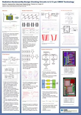
Radiation-Hardened-By-Design Clocking Circuits in 0.13 μmCMOS Technology Yang You1, Jinghong Chen1, Datao Gong2, Deping Huang1, Tiankuan Liu2, Jingbo Ye21Department of Electrical Engineering, Southern Methodist University, Dallas, Texas, 75205 2Department of Physics, Southern Methodist University, Dallas, Texas, 75205 Motivation Radiation-Hardened PLL PLL Vctr Compensation Solution DLL Duty Cycle Correction Circuit Fig.8 Compensation Solution for SET at the PLL CP output (a) Fig.14 (a) Duty cycle detection circuit (b) Duty cycle detection principle Physically Separate 8 Sensitive Transistor Pair (b) Fig.1 (a) Single Event Effects (SEE) [Raoul Velazco] (b) SEE on the timing circuit (DLL) Fig.9 Compensation Result • A result of the interaction between the radiation and the electronic device is SEE • The incident particle generates a dense track of electron hole pairs and cause a transient current pulse • In the timing circuits (such as DLL), SEE will cause a state flip to the digital logic and the delay units in the VCDL • A radiation strike can cause the DLL to lose lock, which results in the loss of synchronization and incorrect data transmission Fig.15 Radiation-hardened duty cycle corrector Fig.4 DICE latch and its layout principle • Dual interlock cell flip-flop is used in designing the phase frequency detector, frequency divider, lock detector, and all other sequential logic blocks to eliminate single event upset • Layouts of the Dice cells are optimized by separating the sensitive transistor pairs physically Fig.10 Output clock jitter comparison for PLL w/woVctrl compensation circuit Fig.16 Duty cycle corrector signal waveforms under SEE Layout and Summary Radiation-Hardened DLL Circuit Solution Fig.5 Split Ring VCO • The voltage-controlled oscillator is designed with two VCOs being cross-coupled to achieve quick recovery by compensating each other during SET Fig.2 12.5 MHz~500 MHz Radiation-Hardened-By-Design Phased-Locked Loop Fig.11 DLL operation procedure • The DLL operation includes a coarse tuning and a find tuning process • Duty cycle correction is needed for the DDR application Fig.17 PLL layout and performance summary Fig.3 267MHz Radiation-Hardened Delayed-Locked Loop Fig.6 VCO tuning ranges, conversion gain and output amplitude • Single-event-hardened phase-locked loop (PLL) for structured-ASIC and digital delay-locked loop (DLL) for DDR2 memory interface applications • The PLL covers a frequency range from 12.5 MHz to 500 MHz with an RMS jitter of 4.7 pS • The radiation-hardened design techniques in the PLL include dual interlock cell flip-flop application, cross-coupled VCOs and charge compensation circuit in the loop filter • The DLL operates at 267 MHz and has a phase resolution of 60 pS • All digital architecture of the DLL makes digital radiation-hardened techniques possible. • The two circuits are hardened against SEEs for charge injection of 250 fC and consume 17 mW and 22 mW of power, respectively • The VCO is designed to cover a octave tuning range from 250 MHz to 500 MHz • Phase noise of the VCO at 1 MHz offset frequency is from -98.9 dBc/Hz to -105 dBc/Hz Fig.12 Radiation hardened-triple modular redundancy (TMR) • Three devices will do the same task and a block selects the most “popular” output • Coarse/Fine PDs and coding logics in this design are protected by TMR Fig.7 VCO control voltage under single event transient effect (PLL is locked) Fig.13 Error correction coding for accumulators • Single event upset is modeled as a 2 mA current pulse with a width of 100 ps • The current pulses are applied to different nodes in the PLL. The VCO control voltage is observed Fig.18 DLL layout and performance summary • Loop filter (accumulator) outputs are thermometer coded and protected by Error Correction Coding • Bubble correction