EML 4561 Introduction to Electronic Packaging
1.36k likes | 2.24k Vues
EML 4561 Introduction to Electronic Packaging. W. Kinzy Jones, Professor MME MWF 11:00-11:50 Jones@fiu.edu 305-393-0506(mobile) 305-348-4663 (office ). Notes on the field. I am Past President and Fellow, IMAPS, The Microelectronics and Packaging Society

EML 4561 Introduction to Electronic Packaging
E N D
Presentation Transcript
EML 4561Introduction to Electronic Packaging W. Kinzy Jones, Professor MME MWF 11:00-11:50 Jones@fiu.edu 305-393-0506(mobile) 305-348-4663 (office)
Notes on the field • I am Past President and Fellow, IMAPS, The Microelectronics and Packaging Society • Research in advanced packaging, 1st Level Assembly, Thermal Management, Components and Electronic Materials- Funded over $7MM in past 15 years • Electronic packaging is a application field that crosses over many disciplines. There are 80,000 ME working in the field. Conferences/journals by ASME, IEEE, ASM, IMAPS, etc. • All former graduate student hired prior to graduation!
Outline • Technological Drivers • Design Process • Electrical Consideration • Mechanical Constraints • Thermal Management • Material Science Fundamentals • Interconnect Technology • Laminate technology • Ceramic Processes ( thick film, cofire ceramic) • Thin Film Deposited
Outline (Cont.) • Components • Active components technologies • Passive Components technologies • IC Packaging ( from DIP to System-on-package (SOP)) • Assembly • First Level Assembly ( wire bonding, flip chip) • Soldering • Manufacturing Processes • Reliability • MIL Standards • Reliability Projections
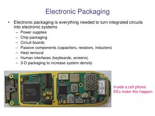
Definition of Packaging IC Board Packaging is a Bridge from IC to System • It Controls: • >90% size • Performance • Cost • Reliability
System Packaging Involves Electrical, Mechanical and Materials Technologies
Trend to Convergent Microsystems Packaging Photonics Microelectronics Convergent Microsystems Discrete Systems RF MEMS Bioelectronics Past Future
Trend to Convergent Systems Convergent Systems Transistors / chip WW S/C Revenue ($B) 10000 • All businesses, people, objects • Network computing • Wide area / bandwidth • Graphical, voice, multimedia, etc. • Many vendors / platforms 100B 10B 1000 1B • Wireless • Wired PCs / Servers 100M Internet 100 10M Mainframes • Businesses & some people • Client-server computing • Local area connection • Text/graphical interface • Many vendors / few architectures 1M 10 PCs 100K • Businesses • Host-based computing • Mainframe • Dumb terminal • Few vendors / architecture 10K 1 1K 2015 1975 1995 Today Year Source: Russ Lange, IBM Microelectronics
What are Convergent Microminiaturized Microsystems (CMM)? • Convergent: Two or more functions • Microminiaturized: >1000x volume reductions • Microsystems: systems with micro-scale technologies
CONSUMER ELECTRONICS MEDICAL Medical Implant/ Diagnostic Monitor/ Communicator Video Cell Phone Trend to Convergent Microminiaturized Systems (CMM) • Functional • Data and Voice • Technology • Digital, RF, Analog and Optical • Product • Computer, consumer and telecom
Moore’s Law Cu - low K SOC Advances SiGe SOI
Integration RF Limits Fundamental Digital Limits SOC Challenges Major Delay Problems Summary • Fundamental • Design & Verification Complexity • Test Complexity • Process Complexity • Mixed Function Costs • Wafer Fab Costs • Legal Problems • Time-to-market
SOC: Integration of Two or More Mixed Functions in a Single IC (a) (b)
What is Wrong with Current Packaging for Tomorrow’s Needs? Bulky Size Higher Cost Cellular Phone Weight Trend • Active ICs 10% • Passives: 90% Lower Performance Poorer Reliability • IC: PPB • Systems Pkg: PPM Barrier to all future systems
What is SOP, SIP, or Board? Package Flash RAM IC mP Stacked IC (Amkor) Package (Fujitsu) Super IC Stack (ASET) RF IC Digital IC Optical IC Substrate A.) Today’s Board: Interconnect Components B.) SIP: Stacked Chip/Package for Reduced Form Factors 3-D ICs IC RF IC Opto IC Digital IC RF Opto Electrical Package with Opto, RF, Digital Functions C.) SOP: Optimizes Functions Between ICs and Package
What are SOC, SIP, and SOP? • SOC: System on Chip • Highly integrated and mixed signal IC with partial system functions in one component • SIP: System in Package • 3-D IC or Package Assembly • Requires Systems Board • SOP: System on Package • Microminiaturized system-level board with two or more embedded RF, digital, analog and optical functions • Best of on-chip and package integration for cost, performance, size and reliability • Similar to SOC but total system function in a microminiaturized board
SOP: SIP + SOC+Systems Board SIP SOP • 3 -D Stacking of ICS or Package Structures, Similar to PWB • Macro dimensions • Vertical stack up • Testable • 3 -D Build up, similar to IC Fabrication • Micro to Nano dimensions • Sequential build up and test similar to MCM-D and IC • Wafer to IC concept for high yield MEMS SIP Ga-As SOC MEMS Ga-As SOC SIP
Why SOP? • SOC is complex to design and test, expensive to Fabricate, long time-to-market and presents fundamental limits. • IC company’s dream for decades. No complete system has been shipped to date. • SOP optimizes the best of IC and package integration for cost, performance, size and reliability. • Faster turn-around and faster time-to-market. • Provides full system solution today that SOC provides tomorrow. • SIP is a 3-D IC or package, not a complete system
Information Technology is a Trillion $ Industry Microsystems & Packaging is 25% of IT Industrial & Medical 11% $105B Automotive 5% $ 48B Military 9% $ 8.7B Consumer 26% $112B Business Equip 38% $ 383B Communications 26% $ 259B Source: Prismark
MSP Market ($320 B) Opto & MEMS ($30B) Microelectronics ($165B) Systems Packaging ($125B)
Information Technology and Microsystem Markets Billion $/Year
Core Technologies • Substrates, circuit boards • Interconnect • Passive components • Active components • Packaging • Traditionally these were treated as discrete elements • Advanced applications require integrated approach of System Level Packaging
Substrates and Circuit Boards • Printed Circuit Board (PCB), Printed Wiring Board (PWB) • Epoxy-glass composite, copper • FR-4, FR = fire retardant • Advanced Resins • Polyimide • BT = bismaleimide traizine • CE = cyanate ester • Ceramic substrates • Aluminum oxide, aluminum nitride, beryllium oxide, glass-ceramic • Interconnect metals - W, Mo, Au, Cu, Ag • Multichip Modules • MCM-D,C,L • Platform • Support interconnect and components • Thermal path away from ICs • Withstand mechanical stresses and vibrations
Microelectronic Density Trends microprocessors logic
I/O Density Trends Chip
Assembly Processes • Board Fabrication • Single layer • Multilayer • PCB • Flex • Ceramic • Populating the board • Pick and place • Insertion • Die attach • Soldering • Solder paste reflow • Wave solder • Solder bump reflow • Encapsulation
CMOS Device Trends Buda et al, 42 CPMT, pp36-41, 1992
NEMI Roadmap, 1996 Packaging trends in Consumer Electronics Packaging trends in Automotive Electronics
NEMI Roadmap for Packaging Trends in High-Performance Systems
Interconnect Density, Std. PWB .1mm = 4 mils
