Download
1 / 1
10 likes | 169 Vues
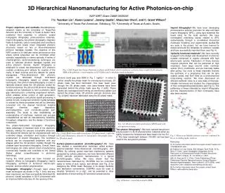
Fig. 4 Photonic crystal fabricated by SFIL. Fig. 1 (left) Single laser beam illuminates a phase mask behind which interference patterns form; (right) Field emission SEM of the photonic crystal template in SU-8 fabricated with phase-mask techniques.

E N D
Fig. 4 Photonic crystal fabricated by SFIL. Fig. 1 (left) Single laser beam illuminates a phase mask behind which interference patterns form; (right) Field emission SEM of the photonic crystal template in SU-8 fabricated with phase-mask techniques Fig. 2 (left) Multi-beam diffraction from a 2D phase mask; (right) the fabricated 3D photonic structure by holographic lithography using the 2D phase mask. Fig. 5 Photocross-linkable polymer structure confirmed by X-ray crystallographic analysis. Fig. 3 A 3D structure fabricated using a SPAN mask with one aperture missing 3D Hierarchical Nanomanufacturing for Active Photonics-on-chip NSF NIRT Grant CMMI-0609345 PIs: Yuankun Lin1, Karen Lozano1, Jeremy Qualls1, Shaochen Chen2, and C. Grant Willson2 1University of Texas-Pan American, Edinburg, TX; 2University of Texas at Austin, Austin, Project objectives and methods--Interdisciplinary research teams at the University of Texas-Pan America and the University of Texas at Austin have combined their expertise in photonic crystal holographic lithography, photo-sensitive materials, imprint lithography, two-photon lithography, magnetic fields & materials, carbon nanotubes and nanofibers to design and create novel integrated photonic structures based on two or three-dimensional photonic bandgap crystals. The objective of this NIRT project is to fabricate active photonics-on-chip where optical properties can be controlled either optically, magnetically or electro-optically. A series of interdisciplinary nanomanufacturing techniques are used to fabricate photonic bandgap crystals and active photonic devices. Imprint lithography is employed to create two-dimensional (2D) photonic crystals containing point defects for creation of the cavity of laser sources and line defects for planar waveguides. Three-dimensional (3D) photonic crystals are fabricated through multi-beam holographic lithography based on phase mask techniques. Two-photon stereolithography is used to fabricate defects inside the 3D photonic crystal for functional devices. The 2D and 3D photonic bandgap crystals will be hybridized to form a photonic band gap heterostructure containing engineered defects, which enables active control of light generation, photon propagation, and photon signal processing in optical circuits. A polymeric photonic crystal template is created by these processes and will be ultimately converted into the desired functional material through chemical vapor deposition, electrodeposition, and microfluidic-guided self-assembly. The study is also establishing an understanding of interfaces, material and process compatibilities as well as manufacturing feasibility, throughput, integration, and the design of functional component. The phase-mask-aided holographic lithography takes advantage of standard tools of the electronic industry, making the process industrially attractive. The desired 2D defects can be engineered with well controlled shape, orientation and location through employment of imprint lithography. The functional defects can be incorporated anywhere with any shapes within the 3D photonic crystals through the ultrafast laser two-photon lithography. Overall, these technologies can make optical circuit manufacturing commercially feasible and contribute to the United States' global competitiveness in photonics technology. During the initial period we have focused our research efforts on holographic lithography, imprint lithography, synthesis of functional electro-optic polymer, and two-photon polymerization. Holographic lithography1--Through laser phase mask techniques (as shown in Fig. 1 (left)) and two laser exposures, we have successfully fabricated 3D photonic crystal templates in SU-8 photoresist with an improved lattice structure for the opening of the Imprint lithography4--We have been developing photosensitive polymer precursor for step and flash imprint lithography (SFIL), using rigid materials like fused silica for the mold element. We have investigated underlying issues related to SFIL systematically through a coordinated theoretical multiscale modeling and experimental studies.We are early in the project, but we have learned to design and build the templates for photonic crystals and have successfully imprinted them (see Fig. 4). Optically functional materials4--We have currently engaged in the design and development of photonic crystals comprised of organic elements with high electro-optic activity. Fabrication of these devices requires polymers that can be patterned at high resolution, have large second order nonlinear optical (NLO) coefficients, and are thermally stable after poling. Our route to these materials involves the synthesis of a prepolymer that can be spin coated, poled, and then fixed by a photochemical cross-linking reaction. We have discovered an efficient synthetic route to a new class of biscross-linkable monomers and studied the characteristics of their corresponding prepolymers (see Fig. 5). The patterning of these materials by imprint lithography and the characterization of their nonlinearity have also been studied. photonic band gap (see SEM in Fig. 1 (right)).2In order to further simplify the phase mask for one-exposure process, 2D phase mask has been fabricated. One laser beam goes through the 2D phase mask, nine laser beams have been generated behind the phase mask (see Fig. 2 (left)). These beams are overlapped and forming an interference pattern just behind the phase mask. 3D photonic periodic structure (see Fig. 2(right)) has been fabricated using the 2D phase mask. Two-photon lithography1--We have realized two-photon polymerization in SU-8 photosensitive materials when we tightly focused the femtosecond laser beam into the SU-8. The laser wavelength between 720-800 nm has been used for the two-photon process. References [1] For further information about this project contact Yuankun Lin <linyk@panam.edu> [2] Yuankun Lin, Isai Olvera, Kris Ohlinger, Zsolt Poole, Di Xu, Kevin P. Chen, “Laser Holographic Lithography for the Fabrication of 3-Dimensional Periodic Photonic Structures”, ICALEO 2007, Orlando, FL, Oct 29-Nov.1, 2007. [3]D. B. Shao and S. C. Chen, “Direct Patterning of Three-Dimensional Periodic Nanostructures by Surface-Plasmon-Assisted Nanolithography”, Nano Letters 6, 2279 (2006), email Shaochen Chen <shaochen.chen@engr.utexas.edu> [4] For further information about this project contact Grant Willson <willson@che.utexas.edu> Surface-plasmon-assisted photolithography3--We have also studied a nanofabrication technique called surface-plasmon-assisted three-dimensional nanolithography (3D-SPAN). By utilizing optical near-field interference patterns generated by surface plasmons, we have fabricated different 2D/3D periodic polymeric nanostructures in a typical photolithography setup. We have shown that the nanostructures fabricated by 3D-SPAN can be controlled easily in terms of size, layout, and defects (see Fig. 3) by designing the SPAN mask. Because of its design flexibility and fabrication convenience, 3DSPAN could be used to develop “photonics on a chip”, and be extended to other applications of direct-writing 3D functional nanostructures.